Data Cache
MOTOROLA
MPC823e REFERENCE MANUAL
10-9
DATA CACHE
10
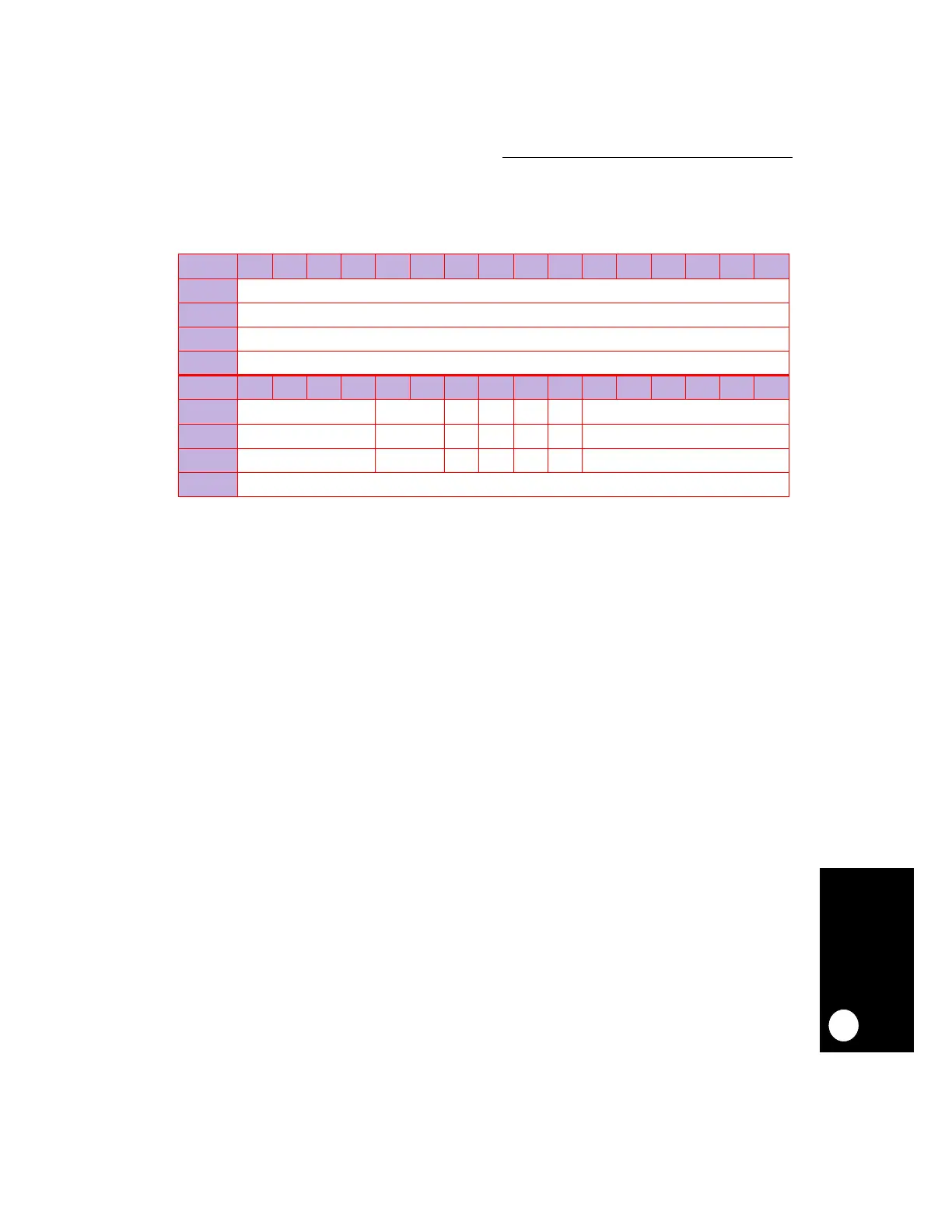
following table illustrates the DC_DAT register’s bit layout when reading a tag. Writing to
DC_DAT is illegal and can result in an undefined data cache state.
TAG—Tag Selection
This field contains the upper 20 bits of the address.
Bits 20–21 and 26–31—Reserved
These bits are reserved and must be set to 0.
V—Valid Cache Line
0 = Entry is not valid.
1 = Entry is valid.
L—Lock Entry
0 = Cache entry is unlocked.
1 = Cache entry is locked.
LRU—Least Recently Used
0 = This entry is not aged or least-recently used.
1 = This entry is aged or least-recently used.
D—Dirty or Clean Cache Line
0 = This entry has not been modified since it was read from memory.
1 = This entry has been modified since it was read from memory.
DC_DAT (TAG READ FORMAT)
BIT
0 1 2 3 4 5 6 7 8 9 10 11 12 13 14 15
FIELD
TAG
RESET
—
R/W
R/W
SPR
570
BIT
16 17 18 19 20 21 22 23 24 25 26 27 28 29 30 31
FIELD
TAG RESERVED V L LRU D RESERVED
RESET
— — ———— —
R/W
R/W R/W R/W R/W R/W R/W R/W
SPR
570
NOTE: — = Undefined.