Memory Controller
15-12 MPC823e REFERENCE MANUAL MOTOROLA
MEMORY CONTROLLER
15
AM—Address Mask
This read/write field provides masking on any corresponding bits in the associated base
register. By masking the address bits independently, external devices of different size
address ranges can be used. Any cleared bit masks the corresponding address bit and any
set bit causes the corresponding address bit to be used in address pin comparison. The AM
field can be set or cleared in any order in the field, thus allowing a resource to reside in more
than one area of the address map.
ATM—Address Type Mask
This field masks certain bits in an address type, thus allowing more than one address space
type to be assigned to a chip-select. Any set bit causes the corresponding address type
code bits to be used as part of the address comparison. Any cleared bit masks the
corresponding address type code bit. The ATM field must be cleared so that address type
codes are ignored as part of the address comparison.
CSNT—Chip-Select Negation Time/SAM—Start Address Multiplex
This bit is used for the GPCM and the SAM bit is used for the UPM. The CSNT bit, in
conjunction with ACS and TRLX, is used to control negation of the CSx
and WEx signals
during an external memory write access handled by the general-purpose chip-select
machine. This function provides extended address/data hold time for slower memories and
peripherals. See Table 15-2 (page 15-28) for more information.
The SAM bit determines the address output on the first cycle of an external memory access.
0 = Address pins reflect the address requested by the internal master.
1 = Address pins reflect the address requested by the internal master multiplexed
according to the AMA field (if UPMA is selected to control the memory access) or
the AMB field (if UPMB is selected).
OR
x
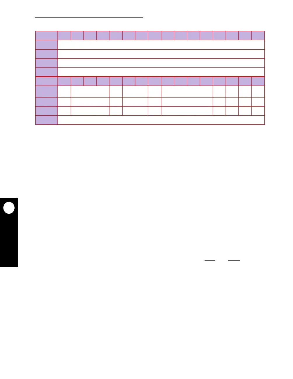
BIT 0 1 2 3 4 5 6 7 8 9 10 11 12 13 14 15
FIELD
AM
RESET
0
R/W
R/W
ADDR
(IMMR &
0x
FFFF0000) +
0x
104 (OR0),
0x
10C (OR1),
0x
114 (OR2),
0x
11C (OR3),
0x
124 (OR4),
0x
12C (OR5),
0x
134 (OR6),
0x
13C (OR7)
BIT 16 17 18 19 20 21 22 23 24 25 26 27 28 29 30 31
FIELD
AM ATM
CSNT/
SAM
ACS/G5LA,G5LS BIH SCY SETA TRLX EHTR RES
RESET
0 0 0 0 0 0 0000
R/W
R/W R/W R/W R/W R/W R/W R/W R/W R/W R/W
ADDR
(IMMR &
0x
FFFF0000) +
0x
106 (OR0),
0x
10E (OR1),
0x
116 (OR2),
0x
11E (OR3),
0x
126 (OR4),
0x
12E (OR5),
0x
136 (OR6),
0x
13E (OR7)
NOTE: The reset value of OR0 has predefined values as shown in the boot OR0 register table.