Memory Controller
MOTOROLA MPC823e REFERENCE MANUAL 15-11
MEMORY CONTROLLER
15
Bits 26–30—Reserved
These bits are reserved and must be set to 0.
V—Valid
This bit indicates that the contents of the base and option registers are valid. The CSx
signal
does not assert until this bit is set. An access to a region that does not have this bit set can
cause a bus monitor timeout. After a system reset, the value of this bit in BR0 depends on
the BDIS bit value in the hard reset configuration word, which is described in
Section 4.3.1.1 Hard Reset Configuration Word.
0 = This bank is invalid.
1 = This bank is valid.
15.3.1.2 OPTION REGISTERS. The option registers (OR0-7) contain the address mask
and address type mask bit for address bus comparison. It also includes the CS general field
and all the GPCM parameters. After reset, OR0 is referred to as the Boot OR0 and it has a
special functionality until the first write to OR0.
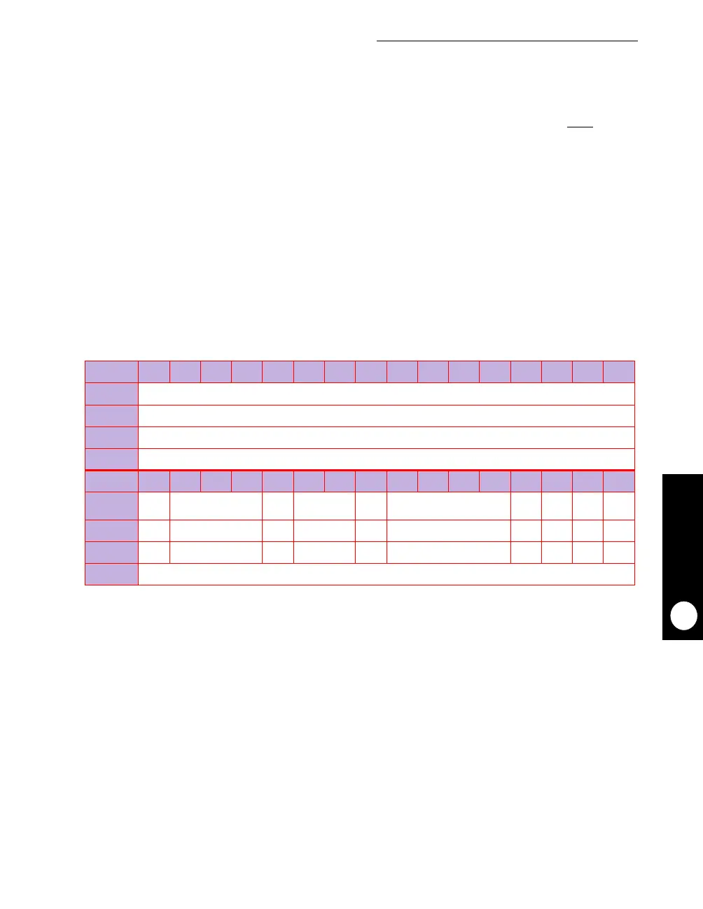
BOOT OR0
BIT 0 1 2 3 4 5 6 7 8 9 10 11 12 13 14 15
FIELD
AM
RESET
0
R/W
R
ADDR
(IMMR &
0x
FFFF0000) +
0x
104
BIT 16 17 18 19 20 21 22 23 24 25 26 27 28 29 30 31
FIELD
AM ATM
CSNT/
SAM
ACS/G5LA,G5LS BIH SCY SETA TRLX EHTR RES
RESET
0 0 1 11 1 1 0100
R/W
R R R R R R RRRR
ADDR
(IMMR &
0x
FFFF0000) +
0x
106