Memory Controller
15-32 MPC823e REFERENCE MANUAL MOTOROLA
MEMORY CONTROLLER
15
The general-purpose chip-select machine also provides a CSNT attribute in the option
register that controls the timing for the appropriate strobe negation in write cycles. When this
attribute is asserted, the strobe is negated one quarter of a clock before the normal case.
For example, when the ACS field equals 00 and CSNT is set, WEx
is negated one quarter
of a clock earlier and when ACS does not equal 00 and CSNT is set, WEx
and CSx are
negated one quarter of a clock earlier. For more information, see Figure 15-6, Figure 15-8,
and Table 15-2.
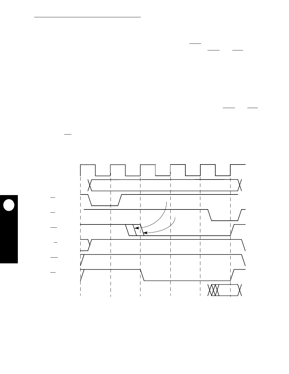
The TRLX field in the option register is provided for memory systems that require more
relaxed timing between signals. When TRLX is set and the ACS field is not equal to 00, an
additional cycle between the address and strobes is inserted by the MPC823e memory
controller, as shown in Figure 15-9.
When TRLX and CSNT are set in a write-memory access, the strobe lines (WEx
and CSx,
if ACS is not equal to 00) are negated one clock earlier than in the normal case, as shown
in Figure 15-11. When a bank is selected to operate with external transfer acknowledge
(SETA and TRLX are set), the memory controller does not support external devices that
provide the TA
signal to complete the transfer with zero wait states. The minimum access
duration in this case is three clock cycles.
Figure 15-9. MPC823e GPCM–Relaxed Timing–Read Access
(ACS = 10 or 11, SCY = 1, and TRLX = 1)
CLOCK
ADDRESS
TS
TA
CSx
R/W
WEx
DATA
OE
ACS = 10
ACS = 11
 Loading...

