Memory Controller
MOTOROLA MPC823e REFERENCE MANUAL 15-37
MEMORY CONTROLLER
15
15.4.1.3 BOOT CHIP-SELECT OPERATION. Boot chip-select operation allows address
decoding for a boot ROM before system initialization occurs. The CS0
signal is the boot
chip-select output and its operation differs from the other external chip-select outputs on
system reset. When the MPC823e internal core begins accessing memory at system reset,
CS0
is asserted for every address, unless an internal register is accessed.
The boot chip-select provides a programmable port size during system reset by using the
BPS field of the hard reset configuration word, as shown in Section 4.3.1.1 Hard Reset
Configuration Word. Setting these appropriately allows a boot ROM to be located
anywhere in the address space. The boot chip-select does not provide write protection and
responds to all address types. CS0
operates this way until the first write to the option register
0 and it can be used as any other chip-select register once the preferred address range is
loaded into base register 0. After the first write to option register 0, the boot chip-select can
only be restarted on system reset. The initial values of the “boot bank” in the memory
controller are described in Table 15-3.
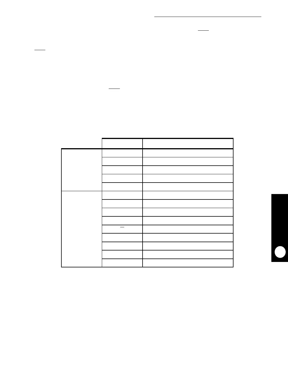
Table 15-3. Boot Bank Field Values After Reset
FIELD VALUE
Base Register 0 PS From Hard Reset Configuration Word
PARE 0
WP 0
MS 00
V From Hard Reset Configuration Word
Option Register 0 AM 00000000000000000
ATM 000
CSNT 1
ACS 11
BI
1
SCY 1111
SETA 0
TRLX 1
EHTR 0