Memory Controller
15-44
MPC823e REFERENCE MANUAL
MOTOROLA
MEMORY CONTROLLER
15
Each of the UPMs can control how the address of the current access is output to the external
pins. Address multiplexing configurations for a specific memory or device can be selected
in the machine mode register. There is also a multiplexing field in the RAM word that is used
to control cycle-by-cycle accesses. Specific user-programmable machine register
information is located in
Section 15.3.1 Register Descriptions
.
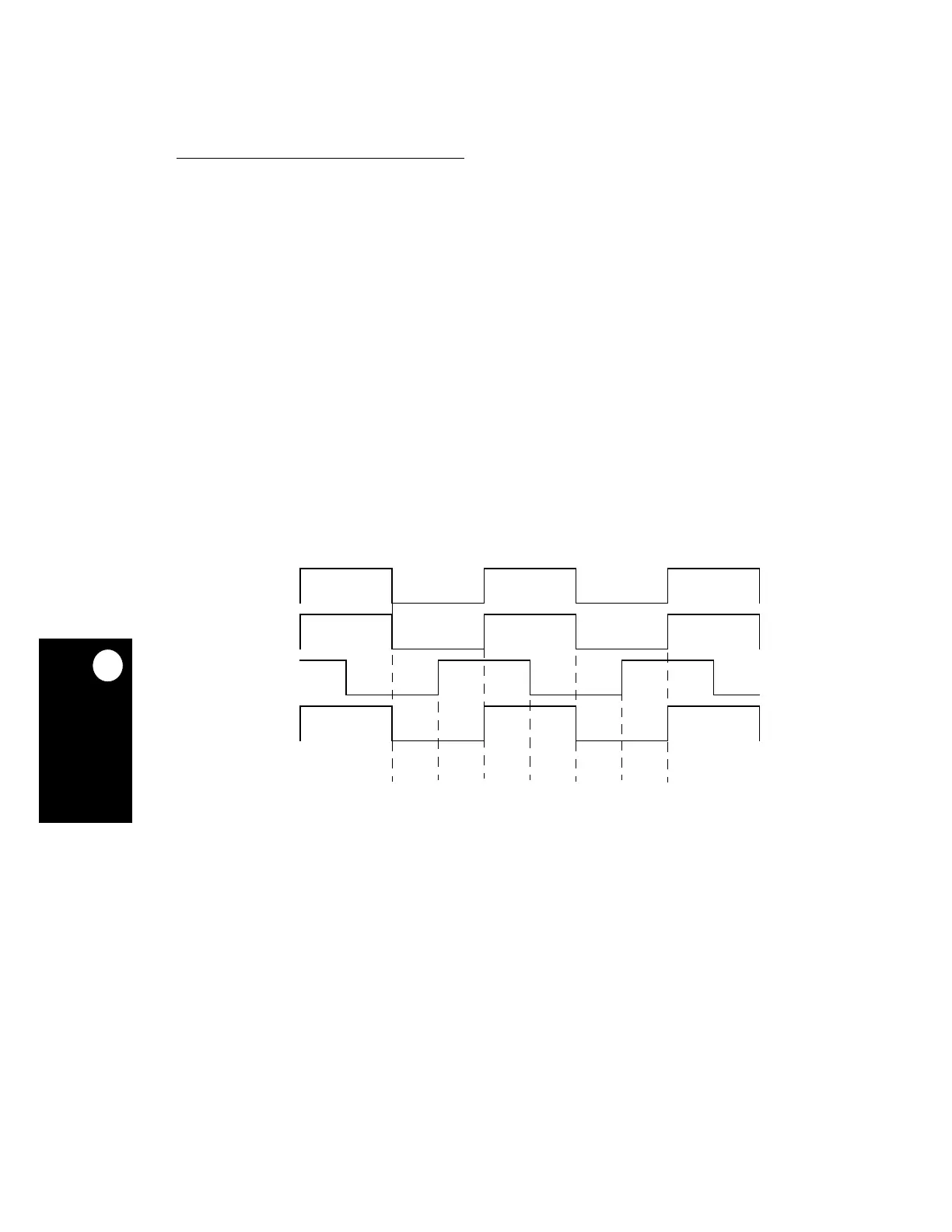
15.5.3 Clock Timing
The RAM word includes fields that specify the value of the various external signals at each
clock edge. The signal timing generator causes the external signals to behave according to
the timing specified in the current RAM word. Figure 15-23 and Figure 15-24 illustrate the
clock schemes of the user-programmable machines in the memory controller. The clock
phases shown in these figures reflect timing windows that specify when generated signals
can change state. Figure 15-23 represents the clock scheme selected when the EBDF field
of the system clock and reset control register is equal to 00. As indicated in the figure,
CLKOUT is the same as system clock. In Figure 15-24, if the EBDF field of the system clock
and reset control register is equal to 01, then CLKOUT is equal to the system clock divided
by 2. Notice that in this scheme GCLK1 does not have a 50% duty cycle. The state of the
external signals may change (if specified in the RAM array) at any edge of GCLK1 and
GCLK2, plus a propagation delay.
Figure 15-23. UPM Clock Scheme One (Division Factor = 1)
CLKOUT
GCLK1
GCLK2
SYSTEM CLOCK
CLOCK PHASE 1 2 3 4 1 2 3