Memory Controller
MOTOROLA
MPC823e REFERENCE MANUAL
15-45
MEMORY CONTROLLER
15
MEMORY CONTROLLER
15
The CSx
signals are handled in a similar way, except that only the CSx signal corresponding
to the currently accessed bank is modified. The BS
signal assertion and negation timing is
also specified for each cycle in the RAM word, but the final value of each one of these
signals depends on the port size of the specified bank, the external address accessed, and
the value of the TSIZx pins.
Figure 15-25 and Figure 15-26 provide examples of how to control the timing of the CSx
,
GPL1
, and GPL2 signals. A RAM word is read on the rising edge of every GCLK2 cycle or
in phase 3 of the previous clock cycle. It determines the value of the CST1–4, G1T3, G1T4,
G2T3, and G2T4 bits, which specifies the timing of chip-selects, byte-selects, and GPLx
signals based on any edge of GCLK1 or GCLK2.
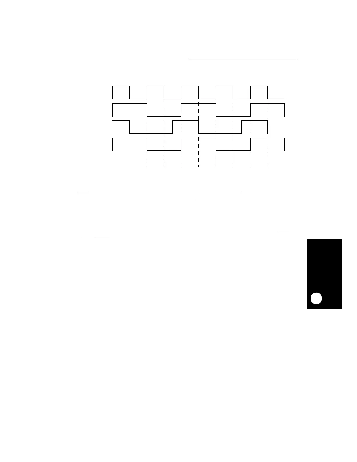
Figure 15-24. UPM Clock Scheme Two (Division Factor = 2)
CLKOUT
GCLK1
GCLK2
SYSTEM CLOCK
1234123
4
CLOCK PHASE