Memory Controller
MOTOROLA MPC823e REFERENCE MANUAL 15-69
MEMORY CONTROLLER
15
MEMORY CONTROLLER
15
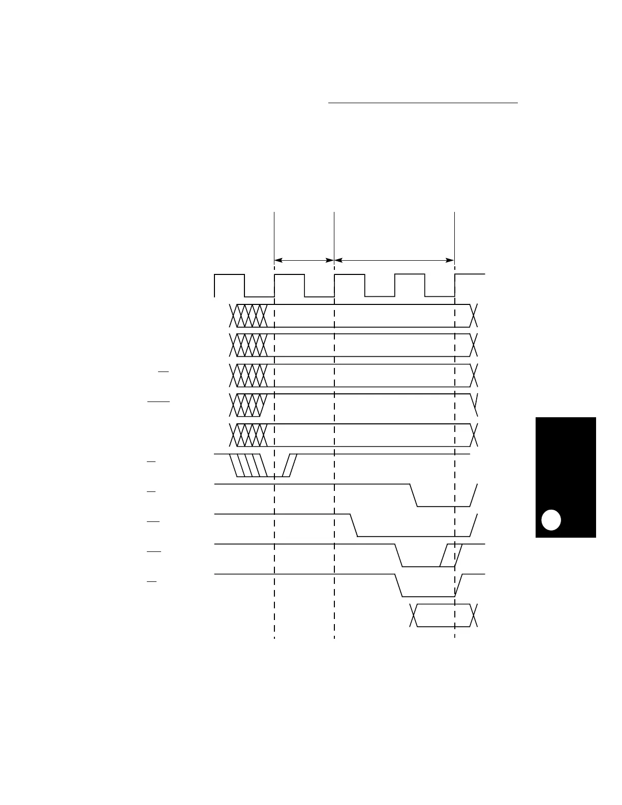
The A[28:20] pins must be used to generate addresses to memory devices during burst
accesses. They duplicate the value of the A[28:20] signals when an internal master initiates
a transaction on the external bus. When an external master initiates a transaction on the
external bus, the A[28:20] pins reflect the value of the A[28:20] pins on the first clock cycle
of the memory access. On subsequent clock cycles, the behavior of the A[28:20] pins
depends on the configuration of the UPM.
Figure 15-35. Synchronous External Master Access
CLKOUT
A[6:27]
CSx
WEx
OE
DATA
TS
TA
ADDRESS
MATCH
AND
COMPARE
MEMORY
DEVICE
ACCESS
RD/
WR
BURST
TSIZEx
A[28:31]