Memory Controller
15-74 MPC823e REFERENCE MANUAL MOTOROLA
MEMORY CONTROLLER
15
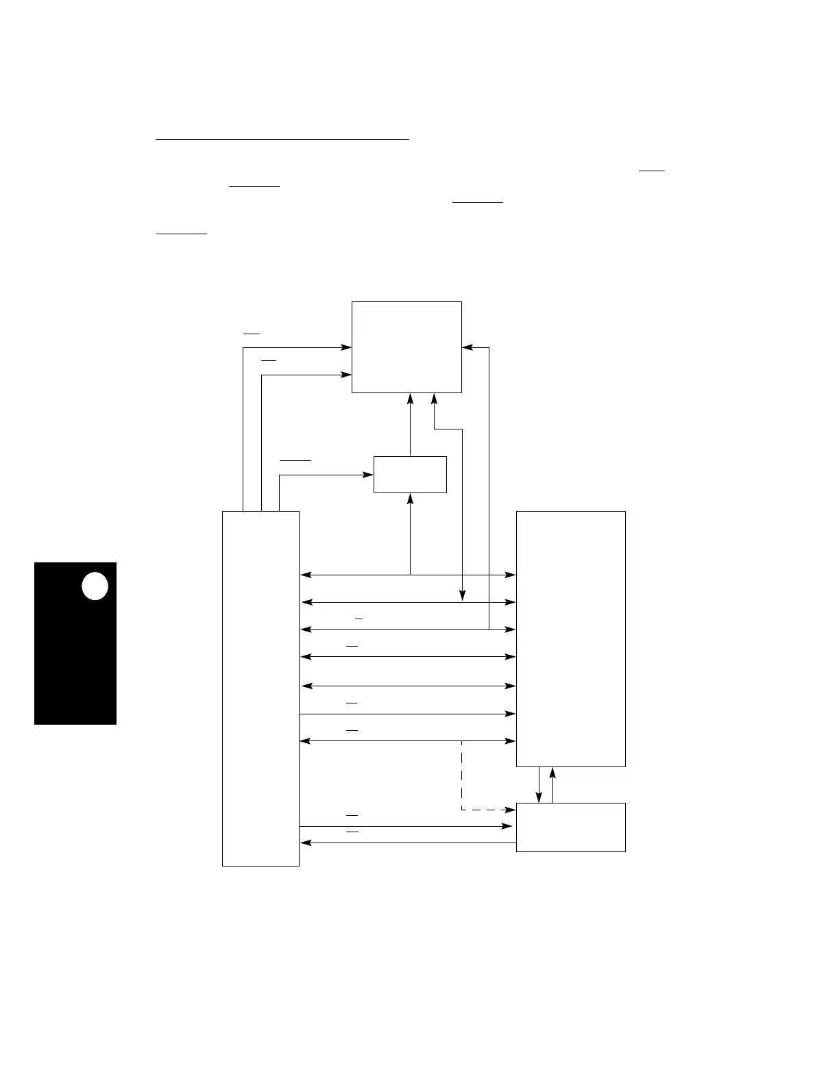
An asynchronous example interconnection in which an external master and the MPC823e
can both share access to a DRAM bank is illustrated in Figure 15-39. Notice that CS1
,
UPMA, and GPL_A5
were chosen to assist in the control of DRAM bank accesses.
Figure 15-40 illustrates the timing behavior of the GPL_A5
and other control signals when
an external master to a DRAM bank initiates a single beat read access. The state of the
GPL_A5
pin in the first clock cycle of the memory device access is determined by the value
of the G5LS bit in the corresponding option register.
Figure 15-39. Asynchronous External Master Interconnect Example
R/W
A[6:31]
BS
x
CS1
AS
D[0:31]
DRAM
MULTIPLEXER
GPL_A5
TA
TSIZx
BR
BG
BB
ARBITRATION
SIGNALS
EXTERNAL
MASTER
EXTERNAL
ARBITER
MPC823e
 Loading...

