Memory Controller
15-76
MPC823e REFERENCE MANUAL
MOTOROLA
MEMORY CONTROLLER
15
15.7 MEMORY SYSTEM INTERFACE EXAMPLES
The following examples illustrate how to connect and set up the UPM RAM array for two
types of DRAM—page mode DRAM and page mode extended data out DRAM. The values
used in these examples apply to either UPMA or UPMB. UPMA is used in the page mode
example and UPMB is used in the extended data out example.
15.7.1 Page Mode DRAM Interface Example
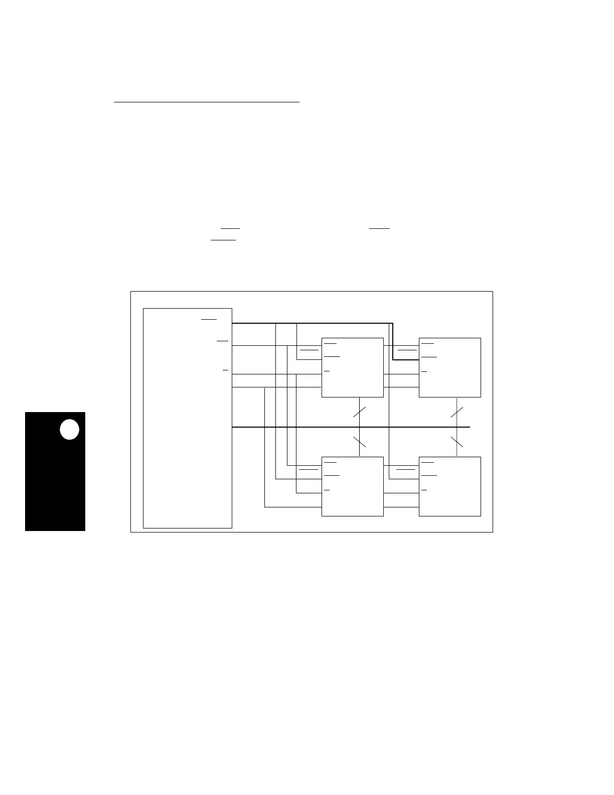
The configuration for a 1M, 32-bit wide memory system using four 256K x 8-bit DRAMs is
illustrated in Figure 15-41. Also shown is the physical connection between UPMA and the
page mode DRAM. The CS1
signal is connected to all the RAS signals and controlled by
the base register. The BS_A
[0:3] signals are mapped one-to-one to each of the four DRAMs
and are controlled by the UPM RAM word. The refresh rate is calculated based on a 25MHz
baud rate generator clock and the DRAM that requires a 512-cycle refresh every 8ms.
Follow these steps to configure a system for page mode DRAM:
1. Determine the system architecture, which includes the MPC823e and the memory
system as shown in the example in Figure 15-41.
2. Use the blank worksheet (Figure 15-58) to draw the timing diagrams for all the memory
cycles associated with your architecture. You can also use, as a reference, the various
timing diagrams in Figure 15-42 through Figure 15-50.
MPC823e
Figure 15-41. Page Mode DRAM Interface Connection
RAS
CAS
x
W
MCM84256
256K x 8
8
A[0:8]
D[0:7]
RAS
CASx
W
MCM84256
256K x 8
8
A[0:8]
D[0:7]
BS_A[0:3]
CS1
R/W
A[21:29]
D[0:31]
RAS
CASx
W
MCM84256
256K x 8
8
A[0:8]
D[0:7]
RAS
CASx
W
MCM84256
256K x 8
8
A[0:8]
D[0:7]
D[0:7] D[8:15]
D[16:23] D[24:31]
BS_A0
BS_A1
BS_A2 BS_A3
 Loading...

