Communication Processor Module
MOTOROLA MPC823e REFERENCE MANUAL 16-27
DSP
COMMUNICATION
16
PROCESSOR MODULE
16.3.2.1 HARDWARE. The RISC microcontroller’s hardware contains special DSP
processing units, such as a multiplier and accumulator that is capable of handling real or
complex numbers, and an address generator that can access cyclic buffer structures in
dual-port RAM.
16.3.2.2 SOFTWARE. Your software interfaces to the DSP via the function descriptor that
is described in system memory. The function descriptor defines the sequence and data flow
of your DSP task.
16.3.2.3 FIRMWARE. The RISC microcontroller’s firmware is a set of DSP functions that
have been compiled to form a library of basic building blocks and each function within the
library is implemented by a microcode routine stored in the internal ROM. In addition, a
software interface is defined that enables parameters to be passed between the core and
communication processor module. Several functions can be chained together to reduce
software intervention and interrupt rates, assuming that all data structures reside in the
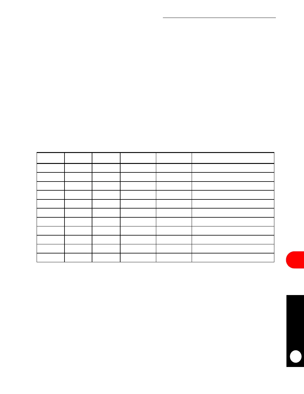
dual-port RAM. Table 16-6 lists the DSP functions that are included in the library.
16.3.3 Programming the DSP Functions
Similar to the serial communication controller buffer descriptor, a function descriptor (FD) is
used to specify the DSP function and pass the parameters. A table of such descriptors forms
a circular queue with a programmable length. The descriptors are stored in external
memory. There are two function descriptor tables (also referred to as chains)—one for the
transmitter and one for the receiver. The core prepares a chain of function descriptors in the
system memory and a special host command notifies the RISC microcontroller when to
execute the chain. A maskable interrupt is generated once the chain is completed. As
illustrated in Figure 16-8, the pointer to the transmit (TX) chain must be written into the
FDBASE field of the DSP2 parameter RAM and the pointer to the receive (RX) chain must
be written into DSP1.
Table 16-6. DSP Functions
FUNCTION OPCODE INPUT COEFFICIENT OUTPUT APPLICATION
FIR1 00001 Real Real Real Decimation, RX Interpolation
FIR2 00010 Complex Real Complex TX Filter, RX Filter
FIR3 00011 Complex Complex Real/Complex EC Computation, Equalizer
FIR5 00011 Complex Complex Real/Complex Fractionally Spaced Equalizer
FIR6 00110 Real Complex Complex —
IIR 00111 Real Real Real Biquad Filter
MOD 01000 Complex Complex Real/Complex TX Modulation
DEMOD 01001 Real Complex Complex RX Demodulation
LMS1 01010 — — — EC Update, Equalizer Update (T/2, T/3)
LMS2 01011 — — — Equalizer Update (2T/3)
WADD 01100 Real — Real Interpolation
 Loading...

