Communication Processor Module
MOTOROLA
MPC823e REFERENCE MANUAL
16-81
COMMUNICATION
16
PROCESSOR MODULE
TIMERS
16.4.2.7 TIMER EVENT REGISTERS.
Each of the 16-bit, memory-mapped timer event
registers (TER1–TER4) are used to report events recognized by the timers. When an output
reference event is recognized, the timer sets the REF bit, regardless of the corresponding
ORI bit in the TMRx register. The capture event is only set if it is enabled by the CE field in
the TMRx register. These registers can be read at any time and are cleared at reset. A bit
is reset by writing a 1 (writing a zero has no effect) and more than one bit can be reset at a
time. However, both bits must be reset before the timer can negate the interrupt to the CPM
interrupt controller.
Bits 0–13—Reserved
These bits are reserved and must be set to 0.
REF—Output Reference Event
This bit signifies that the counter has reached the value in the TRRx register. The ORI bit in
the TMRx register is used to enable the interrupt request caused by this event.
CAP—Capture Event
This bit signifies that the counter value has been latched into the TCRx register. The CE field
in the TMRx register is used to enable generation of this event.
16.4.3 Initializing the Timers
The following is an example of timer 2’s initialization sequence that is required to generate
an interrupt every 10 microseconds, assuming a 25MHz general system clock. An interrupt
must be generated after each 250 system clock.
1. Write 0x0000 to the TGCR. This puts timer 2 into a reset state. Cascaded mode is not
used here.
2. Write 0x001A to the TMR2. This enables the timer’s prescaler to divide by 1 and sets
the clock source to general system clock. It also enables an interrupt to occur when
the reference value is reached and restarts the timer to continuously generate 10ms
interrupts.
3. Write 0x0000 to the TCN2. This initializes the timer 2 count to zero (default state of this
register).
4. Write 0x00FA to the TRR2. This initializes the timer 2 reference value to 250 (decimal).
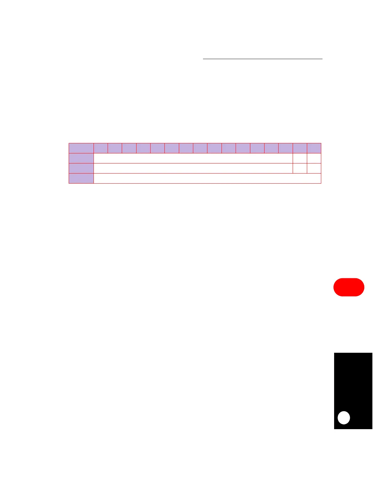
TER1–TER4
BIT
0 1 2 3 4 5 6 7 8 9 10 11 12 13 14 15
FIELD
RESERVED REF CAP
RESET
000
ADDR
(IMMR & 0xFFFF0000) + 0x9B0 (TER1), 0x9B2 (TER2), 0x9B4 (TER3), 0x9B6 (TER4)