Communication Processor Module
MOTOROLA MPC823e REFERENCE MANUAL 16-89
IDMA
COMMUNICATION
16
PROCESSOR MODULE
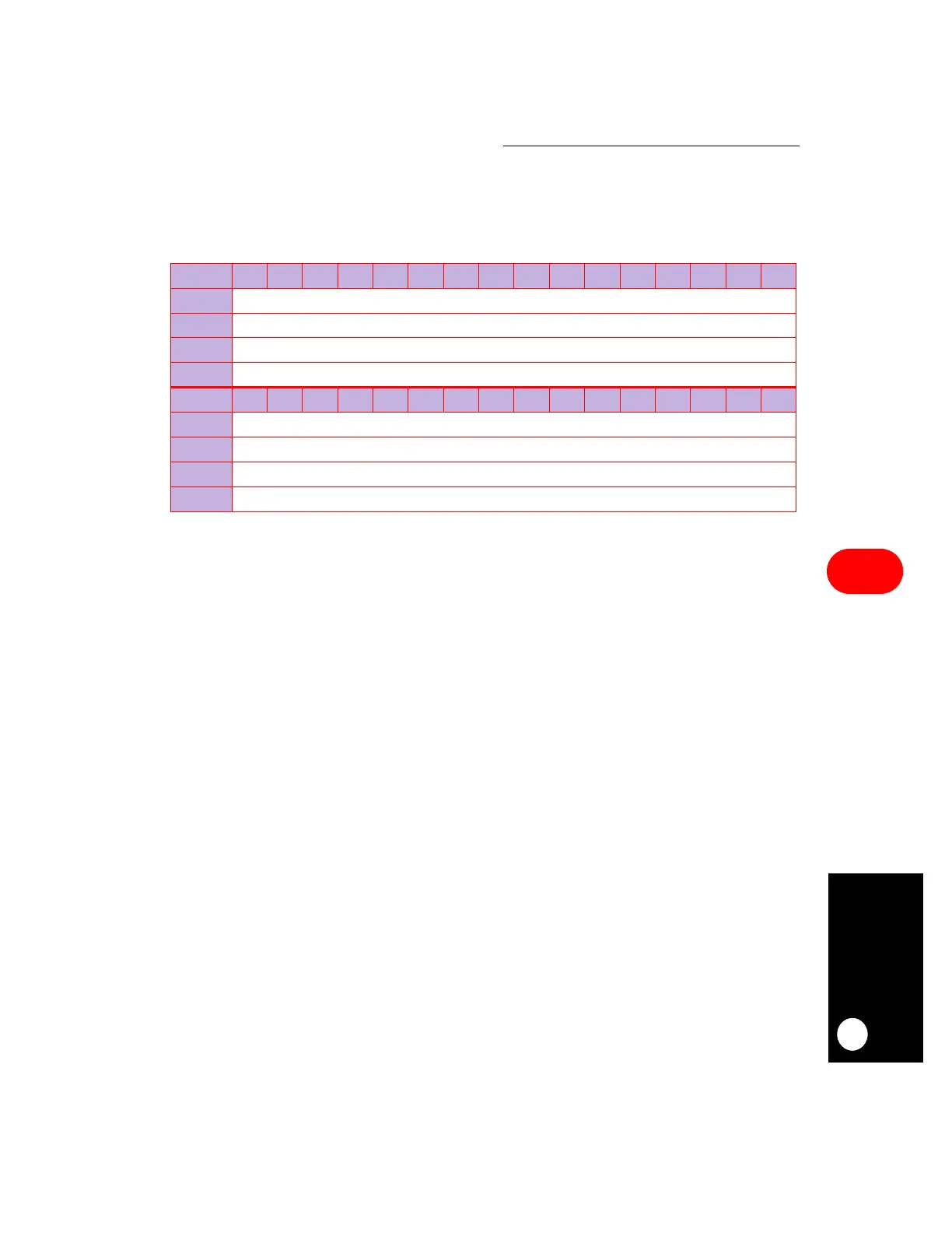
16.5.2.4 SDMA ADDRESS REGISTER. The 32-bit read-only SDMA address register
(SDAR) contains the system address that is accessed during an SDMA bus error. It is
undefined at reset.
SBEA—SDMA Bus Error Address
This field contains the system address accessed when the SDMA encounters a bus error.
16.6 EMULATING IDMA
Using the IDMA-dedicated SDMA channel, which is not part of the 12 channels, the RISC
microcontroller can be configured to provide a general-purpose DMA functionality. Two
general-purpose independent DMA (IDMA) channels are supported. In this special
emulation mode, you can specify any memory-to-memory or peripheral-to-memory transfers
to be implemented in the same way as dedicated DMA hardware.
The general-purpose IDMA controllers operate in different data transfer modes that you are
responsible for programming. They can transfer data between any combination of memory
and I/O. In addition, data can be transferred in byte, half-word, word, or burst quantities and
the source and destination addresses can be odd or even. The most efficient packing
algorithms are used in IDMA transfers. The single address mode performs the best because
it allows data to be transferred between memory and the peripheral within a single bus cycle.
The chip-select and wait-state generation logic on the MPC823e can be used with IDMA.
IDMA supports three buffer handling modes—single buffer, autobuffer, and buffer chaining.
The single buffer mode allows a single buffer peripheral to memory data transfer with single
address (flyby) burst transfers. The autobuffer mode allows blocks of data to be repeatedly
moved from one location to another without you having to intervene. The buffer chaining
mode allows a chain of blocks to be moved sequentially. You specify how to move the data
using buffer descriptors similar to those used by a serial communication controller. These
buffer descriptions reside in the dual-port RAM.
SDAR
BIT 0 1 2 3 4 5 6 7 8 9 10 11 12 13 14 15
FIELD SBEA
RESET —
R/W R
ADDR (IMMR & 0xFFFF0000) + 0x904
BIT 16 17 18 19 20 21 22 23 24 25 26 27 28 29 30 31
FIELD SBEA
RESET —
R/W R
ADDR (IMMR & 0xFFFF0000) + 0x906
NOTE: — = Undefined.