Communication Processor Module
16-122
MPC823e REFERENCE MANUAL
MOTOROLA
SERIAL
I/F
COMMUNICATION
16
PROCESSOR MODULE
16.7.4.5 PROGRAMMING THE SERIAL INTERFACE RAM ENTRIES.
The programming
of each word within the RAM determines the routing of the serial bits and assertion of strobe
outputs. The RAM programming codes are shown in the following table.
LOOP—Loopback
0 = Normal mode.
1 = Loopback mode for this time-slot.
SWTR—Switch Transmit and Receive
This bit is only valid in the receive route RAM and is ignored in the transmit route RAM. This
bit affects the operation of both the L1RXDx and L1TXDx pins. The SWTR bit is only set in
special situations in which you prefer to receive data from a transmit pin and transmit data
on a receive pin. For instance, consider the situation in which devices A and B are
connected to the same time-division multiplex, each with different time-slots. Normally, there
is no opportunity for stations A and B to communicate with each other directly over the
time-division multiplex since they both receive the same TDM receive data and transmit on
the same TDM transmit signal.
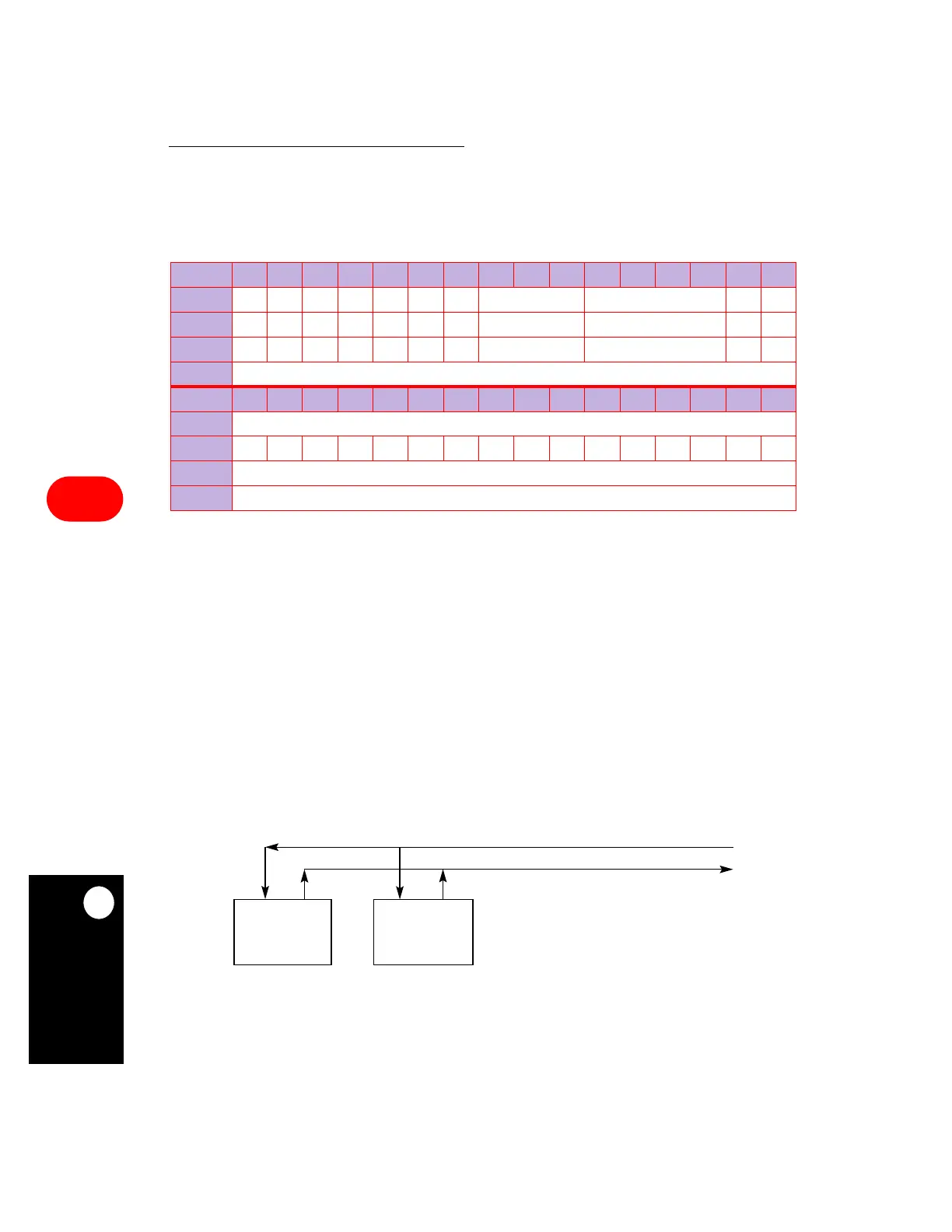
SERIAL INTERFACE RAM ENTRIES
BIT
0 1 2 3 4 5 6 7 8 9 10 11 12 13 14 15
FIELD
LOOP SWTR SSEL1 SSEL2 SSEL3 SSEL4 RES CSEL CNT BYT LST
RESET
0000000 0 0 00
R/W
R/W R/W R/W R/W R/W R/W R/W R/W R/W R/W R/W
ADDR
(IMMR & 0xFFFF0000) + 0xC00 TO 0xDFF
BIT
16 17 18 19 20 21 22 23 24 25 26 27 28 29 30 31
FIELD
RESERVED
RESET
11111111
11
1
111
11
R/W
R/W
ADDR
(IMMR & 0xFFFF0000) + 0xC00 TO 0xDFF
Figure 16-50. Using the SWTR Bit
RX
RX
TX
TX
STATION A
TDM
TRANSMIT DATA
TDM
RECEIVE DATA
STATION B
 Loading...

