Communication Processor Module
MOTOROLA
MPC823e REFERENCE MANUAL
16-129
SERIAL
I/F
COMMUNICATION
16
PROCESSOR MODULE
16.7.5.2 SERIAL INTERFACE MODE REGISTER.
The 32-bit, memory-mapped,
read/write serial interface mode register (SIMODE) defines the serial interface operation
modes and with serial interface RAM allows you to support any or all of the ISDN channels
independently when in IDL or GCI mode.
SMC2—SMC2
Connection
0 = NMSI mode. The clock source is determined by the SMC2CS field and the data
comes from a dedicated SMTXD2 and SMRXD2 pin in NMSI mode.
1 = SMC2 is connected to the multiplexed serial interface (TDM channel).
SMC2CS—SMC2 Clock Source (NMSI mode)
SMC2 can take its clocks from one of the baud rate generators or one of four pins from the
bank of clocks. However, the SMC2 transmit and receive clocks must be the same when
they are connected to NMSI mode.
000 = SMC2 transmit and receive clocks are BRG1.
001 = SMC2 transmit and receive clocks are BRG2.
010 = SMC2 transmit and receive clocks are BRG3.
011 = SMC2 transmit and receive clocks are BRG4.
100 = SMC2 transmit and receive clocks are CLK1.
101 = SMC2 transmit and receive clocks are CLK2.
110 = SMC2 transmit and receive clocks are CLK3.
111 = SMC2 transmit and receive clocks are CLK4.
SMC1—SMC1
Connection
0 = NMSI mode. The clock source is determined by the SMC1CS field and the data
comes from a dedicated pin SMTXD1 and SMRXD1 in NMSI mode.
1 = SMC1 is connected to the multiplexed serial interface (TDM channel).
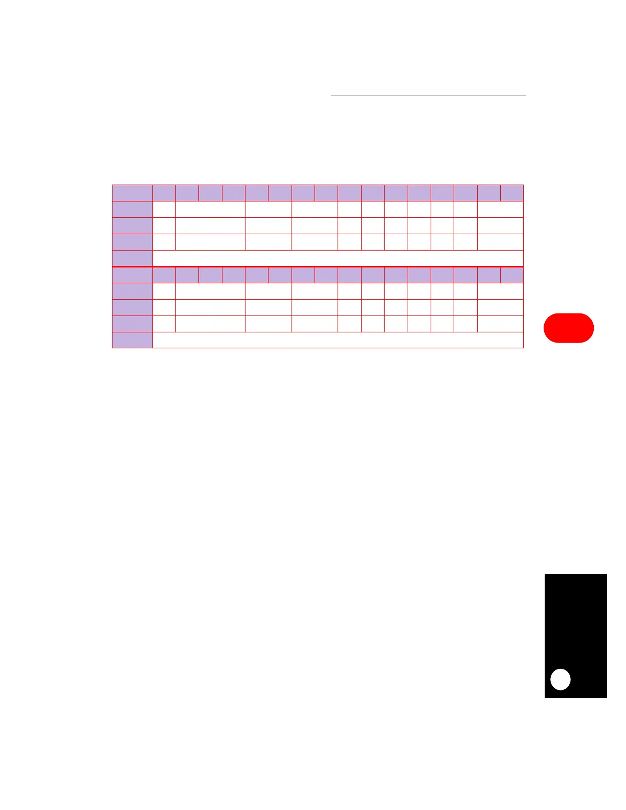
SIMODE
BIT
0 1 2 3 4 5 6 7 8 9 10 11 12 13 14 15
FIELD
SMC2 SMC2CS SDMB RFSDB DSCB CRTB STZB CEB FEB GMB TFSDB
RESET
0 0 0 0 000000 0
R/W
R/W R/W R/W R/W R/W R/W R/W R/W R/W R/W R/W
ADDR
(IMMR & 0xFFFF0000) + 0xAE0
BIT
16 17 18 19 20 21 22 23 24 25 26 27 28 29 30 31
FIELD
SMC1 SMC1CS SDMA RFSDA DSCA CRTA STZA CEA FEA GMA TFSDA
RESET
0 0 0 0 000000 0
R/W
R/W R/W R/W R/W R/W R/W R/W R/W R/W R/W R/W
ADDR
(IMMR & 0xFFFF0000) + 0xAE2