Communication Processor Module
MOTOROLA
MPC823e REFERENCE MANUAL
16-149
SERIAL
I/F
COMMUNICATION
16
PROCESSOR MODULE
16.7.6.2.1 IDL Interface Programming Example.
Using the example in
Section 16.7.6.1 IDL Interface Implementation
as a base model, the initialization
sequence is as follows:
1. Assuming SMC1 is connected to the B1 channel, SMC2 is connected to the B2
channel, and SCC2 is connected to the D channel, program the serial interface RAM.
Write all entries that are not used with 0x0001, set the LST bit, and disable the routing
function.
2. The SIMODE equals 0x80008145. Only TDMA is used. The two SMCs are connected
to the time-slot assigner.
3. The SICR equals 0x0000c000. SCC2 is connected to the time-slot assigner. SCC2
supports the grant mechanism since it is on the D channel.
4. In the PAODR, bit 9 is set to 1. Configure L1TXDA to be an open-drain output.
5. In the PAPAR, bits 9, 8, and 7 are set to 1. Configure L1TXDA, L1RXDA, and
L1RCLKA.
6. In the PADIR, bits 9 and 8 are set to 1. PADIR bit 7 = 0. Configure L1TXDA, L1RXDA,
and L1RCLKA.
7. In the PCPAR, bits 12, 5, and 11 are set to 1. Configure L1RQa, L1TSYNCa, and
L1RSYNCA.
8. In the PCDIR, bit 12 is set to 0. L1RQA is an input. L1TSYNCA performs the L1GRA
function and is therefore an output, but it does not need to be configured with PCDIR
bit 5 is set to 0. L1RSYNCA is an input, but it does not need to be configured with a
PCDIR bit.
9. TheSIGMR equals 0x04. Enable TDMA (one static TDM).
10.The SICMR is not used.
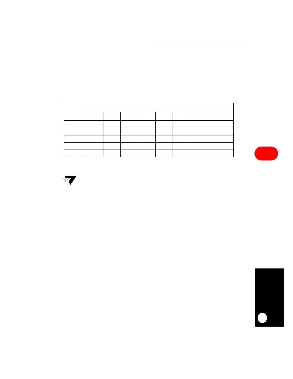
ENTRY
NUMBER
RAM WORD
SWTR SSEL CSEL CNT BYT LST DESCRIPTION
1 0 0000 101 0000 1 0 8 Bits SMC2 (B1)
2 0 0000 010 0000 0 0 1 Bit SCC2 (D)
3 0 0000 000 0000 0 0 1 Bit No Support
4 0 0000 110 0000 1 0 8 Bits SMC2 (B2)
5 0 0000 010 0000 0 1 1 Bit SCC2
Note:
Since IDL requires the same routing for both receive and transmit, an exact
duplicate of the above entries must be written to both the receive and transmit
sections of the serial interface RAM beginning at serial interface RAM addresses
0 and 128, respectively.