Communication Processor Module
16-236 MPC823e REFERENCE MANUAL MOTOROLA
COMMUNICATION
16
SCCs
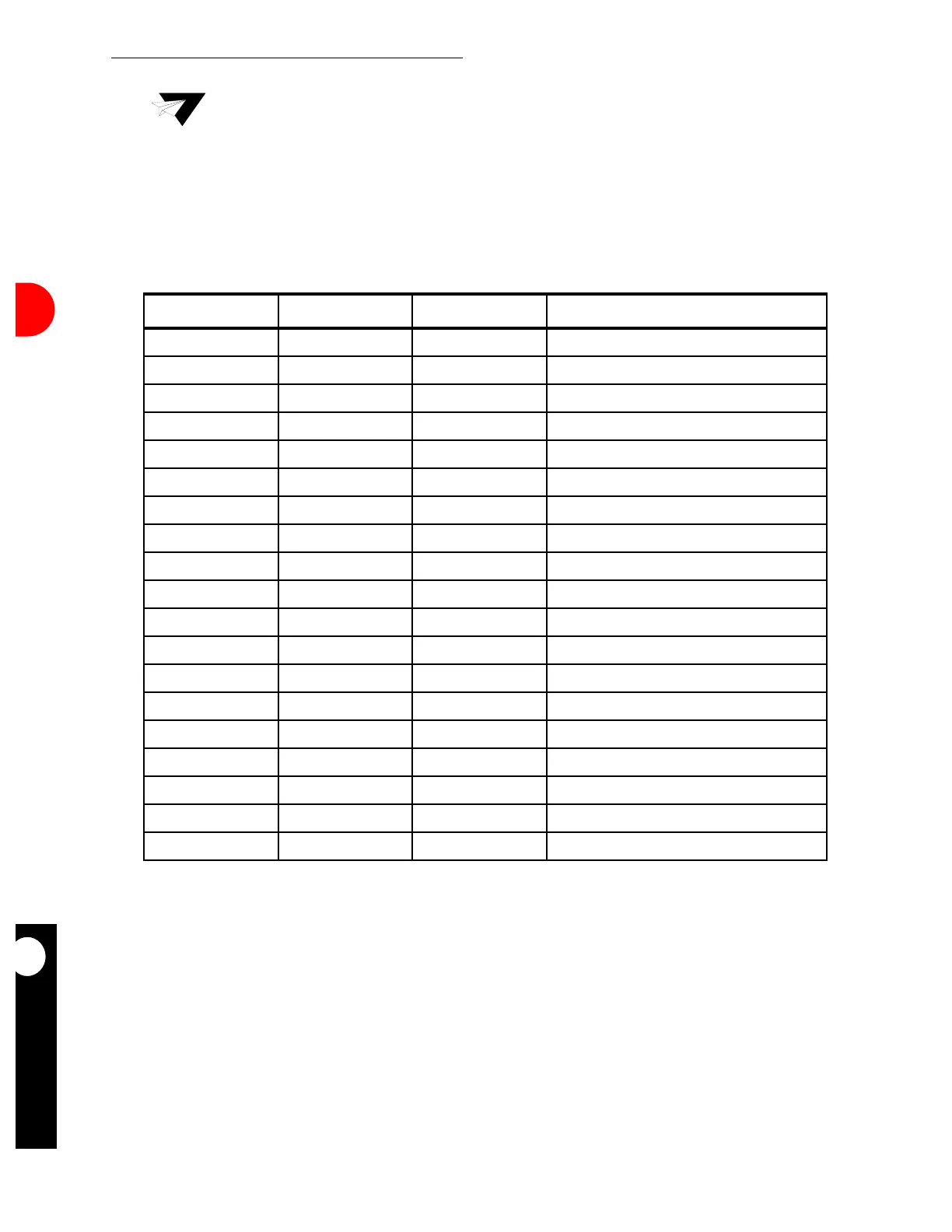
16.9.16.4 SCCx HDLC PARAMETER RAM MEMORY MAP.When configured to operate
in HDLC mode, the serial communication controllers overlay the structure used in Table 16-
24 with the HDLC parameters that are described in Table 16-27 below.
Note: The SCCx HDLC controller must receive a maximum of eight clocks (after a
frame is received) to complete the reception.
Table 16-27. SCCx HDLC Parameter RAM Memory Map
ADDRESS NAME WIDTH DESCRIPTION
SCCx Base + 30 RES Word Reserved
SCCx Base + 34 C_MASK Word CRC Constant
SCCx Base + 38 C_PRES Word CRC Preset
SCCx Base + 3C DISFC Half-word Discard Frame Counter
SCCx Base + 3E CRCEC Half-word CRC Error Counter
SCCx Base + 40 ABTSC Half-word Abort Sequence Counter
SCCx Base + 42 NMARC Half-word Nonmatching Address RX Counter
SCCx Base + 44 RETRC Half-word Frame Transmission Counter
SCCx Base + 46 MFLR Half-word Max Frame Length Register
SCCx Base + 48 MAX_CNT Half-word Maximum Length Counter
SCCx Base + 4A RFTHR Half-word Received Frames Threshold
SCCx Base + 4C RFCNT Half-word Received Frames Count
SCCx Base + 4E HMASK Half-word User-Defined Frame Address Mask
SCCx Base + 50 HADDR1 Half-word User-Defined Frame Address
SCCx Base + 52 HADDR2 Half-word User-Defined Frame Address
SCCx Base + 54 HADDR3 Half-word User-Defined Frame Address
SCCx Base + 56 HADDR4 Half-word User-Defined Frame Address
SCCx Base + 58 TMP Half-word Temp Storage
SCCx Base + 5A TMP_MB Half-word Temp Storage
NOTE:
You are only responsible for initializing the items in bold.
SCCx base = (IMMR & 0xFFFF0000) + 0x3D00 (SCC2) and 0x3E00 (SCC3).
All references to registers in the parameter RAM table are actually implemented in the dual-port RAM
area as a memory-based register.
 Loading...

