External Signals
2-12 MPC823e REFERENCE MANUAL MOTOROLA
EXTERNAL SIGNALS
2
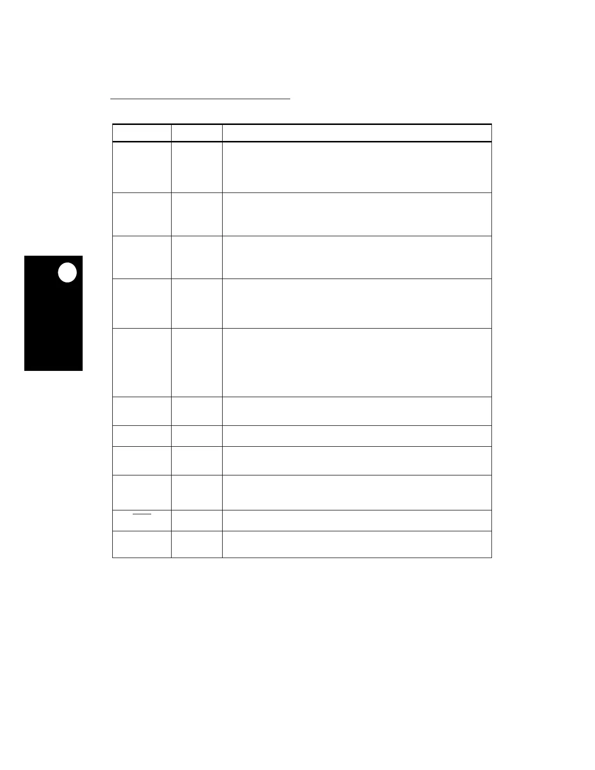
PD[6]
LCD_AC
LOE
BLANK
R1 General-Purpose I/O Port D Bit 6—Bit 6 of the general-purpose I/O port D.
LCD_AC—This output signal from the LCD controller toggles once every
programmable number of frames. It is used with passive panels.
LOE—The output enable signal that is used with TFT panels.
BLANK—The video controller uses this signal to let the video encoder know that the
current cycle is a blank type.
PD[5]
FRAME
VSYNC
P2 General-Purpose I/O Port D Bit 5—Bit 5 of the general-purpose I/O port D.
FRAME—The output signal from the video controller that marks the beginning of a
new frame.
VSYNC—The output signal from the LCD controller that marks the beginning of a
new frame.
PD[4]
LOAD
HSYNC
P3 General-Purpose I/O Port D Bit 4—Bit 4 of the general-purpose I/O port D.
LOAD—The output signal from the video controller that marks the beginning of a
new display line.
HSYNC—The output signal from the LCD controller that marks the beginning of a
new frame.
PD[3]
SHIFT/CLK
CLK
N4 General-purpose I/O Port D Bit 3—Bit 3 of the general-purpose I/O port D.
SHIFT/CLK—This output signal is used to generate the shift clock timing to the LCD
panel when using the LCD controller. The direction is defined when you program it.
CLK—When the video controller is used, the CLK function can either be an output
clock to drive the video encoder or an external input clock from the video encoder to
drive the video controller. The direction is defined when you program it.
Power Supply See Table 2-2
for pin
breakout.
VDDL—Power supply of the internal logic.
VDDH—Power supply of the I/O buffers and certain parts of the clock control.
VDDSYN—Power supply of the phase-locked loop circuitry.
VSSSYN—Power supply of the phase-locked loop ground.
VSSSYN1—Power supply of the phase-locked loop ground.
GND—Power supply ground.
KAPWR—Power supply of the internal oscillator, real-time clock, periodic interrupt
timer, decrementer, and timebase.
TCK
DSCK
T12 Test Clock—This input signal is the clock of the JTAG interface.
Development Serial Clock—This input signal is the clock for the debug port
interface.
TMS R12 Test Mode Select—This input signal controls the TAP machine sequence in the
JTAG interface.
TDI
DSDI
R11 Test Data Input—This input signal is the data in the JTAG interface.
Development Serial Data Input—This input signal is the data for the debug port
interface.
TDO
DSDO
N12 Test Data Output—This three-state output signal is the data out of the JTAG
interface.
Development Serial Data Output—This output signal is the data out of the debug
port interface.
TRST
P11 Test Reset—This input signal is the asynchronous reset of the TAP machine on the
JTAG interface.
N/C See Table 2-2
for pin
breakout.
No Connect—These pins are not connected.
Table 2-1. Signal Descriptions (Continued)
SIGNAL PIN NUMBER DESCRIPTION