Communication Processor Module
MOTOROLA
MPC823e REFERENCE MANUAL
16-479
PORTS
COMMUNICATION
16
PROCESSOR MODULE
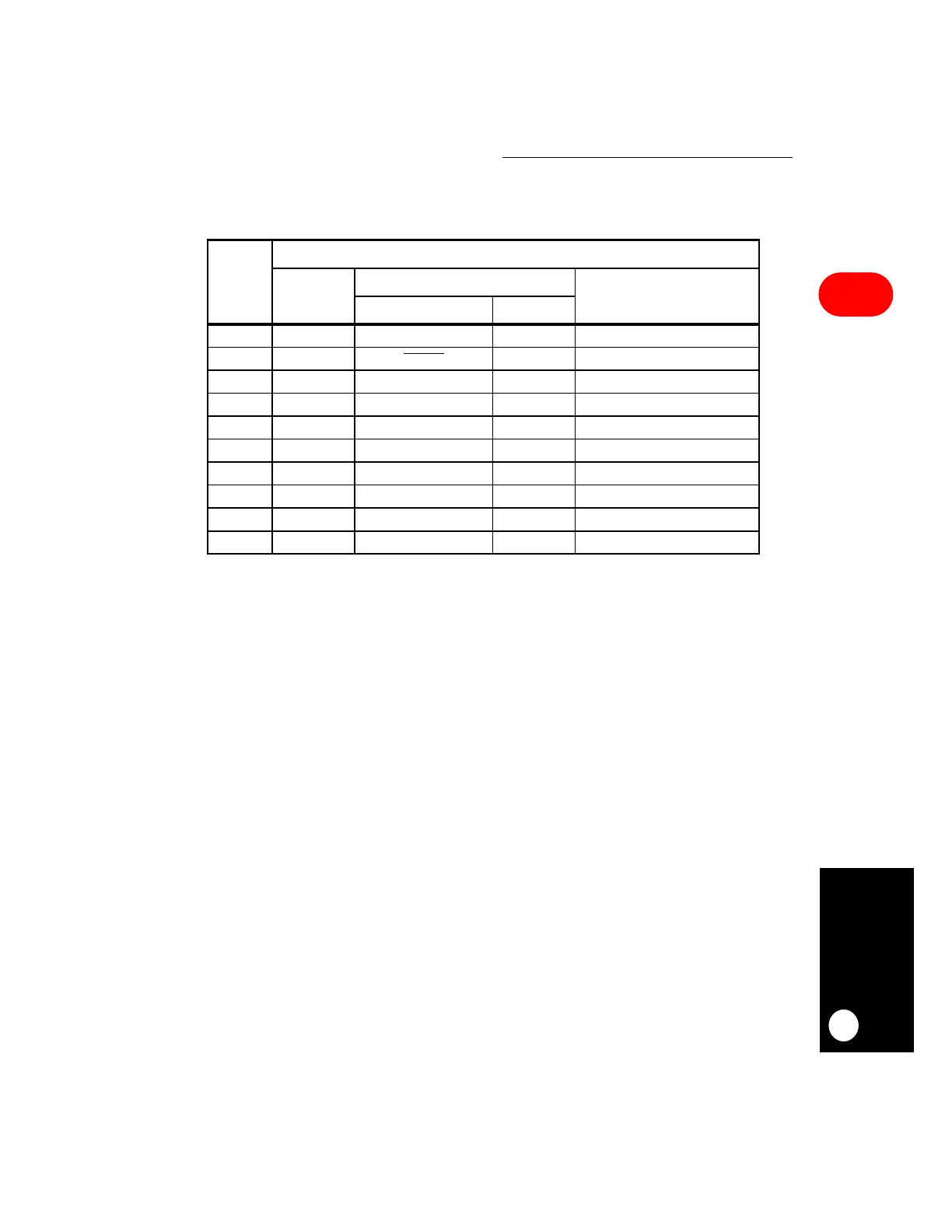
Table 16-41 contains the default description of all port A pin options.
If a port A pin is selected as a general-purpose I/O pin, it can be accessed through the port
A data register (PADAT). Data written to the PADAT is stored in an output latch. If a port A
pin is configured as an output, the output latch data is gated onto the port pin. When PADAT
is read, the port pin itself is read. If a port A pin is configured as an input, data written to
PADAT is still stored in the output latch, but is prevented from reaching the port pin. In this
case, when PADAT is read, the state of the port pin is read. If an input to a peripheral is not
supplied from a pin, then a default value is supplied to the on-chip peripheral as listed in
Table 16-41.
Table 16-41. Port A Pin Assignment
SIGNAL
PIN FUNCTION
PAPAR = 0 PAPAR = 1 PERIPHERALS
PADIR = 0 PADIR = 1
PA15 PORT A15 USBRXD — GND
PA14 PORT A14
USBOE
——
PA13 PORT A13 RXD2 — GND
PA12 PORT A12
TXD2
——
PA9 PORT A9 SMRXD2
L1TXDA
Undefined
PA8 PORT A8 SMTXD2 L1RXDA GND
PA7 PORT A7 CLK1/TIN1/L1RCLKA BRGO1 CLK1/TIN1/L1RCLKA = BRGO1
PA6 PORT A6 TIN3/CLK2/L1RCLKB TOUT1 TIN3/CLK2 = GND
PA5 PORT A5 CLK3/TIN2/L1TCLKA BRGO2 CLK3/TIN2/L1TCLKA = BRGO2
PA4 PORT A4 TIN4/CLK4/L1TCLKB TOUT2 TIN4/CLK4 = GND
NOTE: The items in bold have open-drain capability.
The I/O direction for the TDM and SMC2 pins are reversed. See PA8 and PA9.