Communication Processor Module
MOTOROLA MPC823e REFERENCE MANUAL 16-481
PORTS
COMMUNICATION
16
PROCESSOR MODULE
16.14.3.3 PORT A DATA DIRECTION REGISTER. The port A data direction (PADIR)
register is cleared by system reset.
Bits 0–3—Reserved
These bits are reserved and must be set to 0.
DR4–DR15—Direction Pins 4-15
0 = The corresponding pin is an input.
1 = The corresponding pin is an output.
16.14.3.4 PORT A PIN ASSIGNMENT REGISTER. The port A pin assignment register
(PAPAR) is cleared at system reset.
Bits 0–3—Reserved
These bits are reserved and must be set to 0.
DD4–DD15—Dedicated Peripheral Pins 4-15
0 = General-purpose I/O. The peripheral functions of the pin are not used.
1 = Dedicated peripheral function. The pin is used by the internal module. The
on-chip peripheral function to which it is dedicated can be determined by other bits.
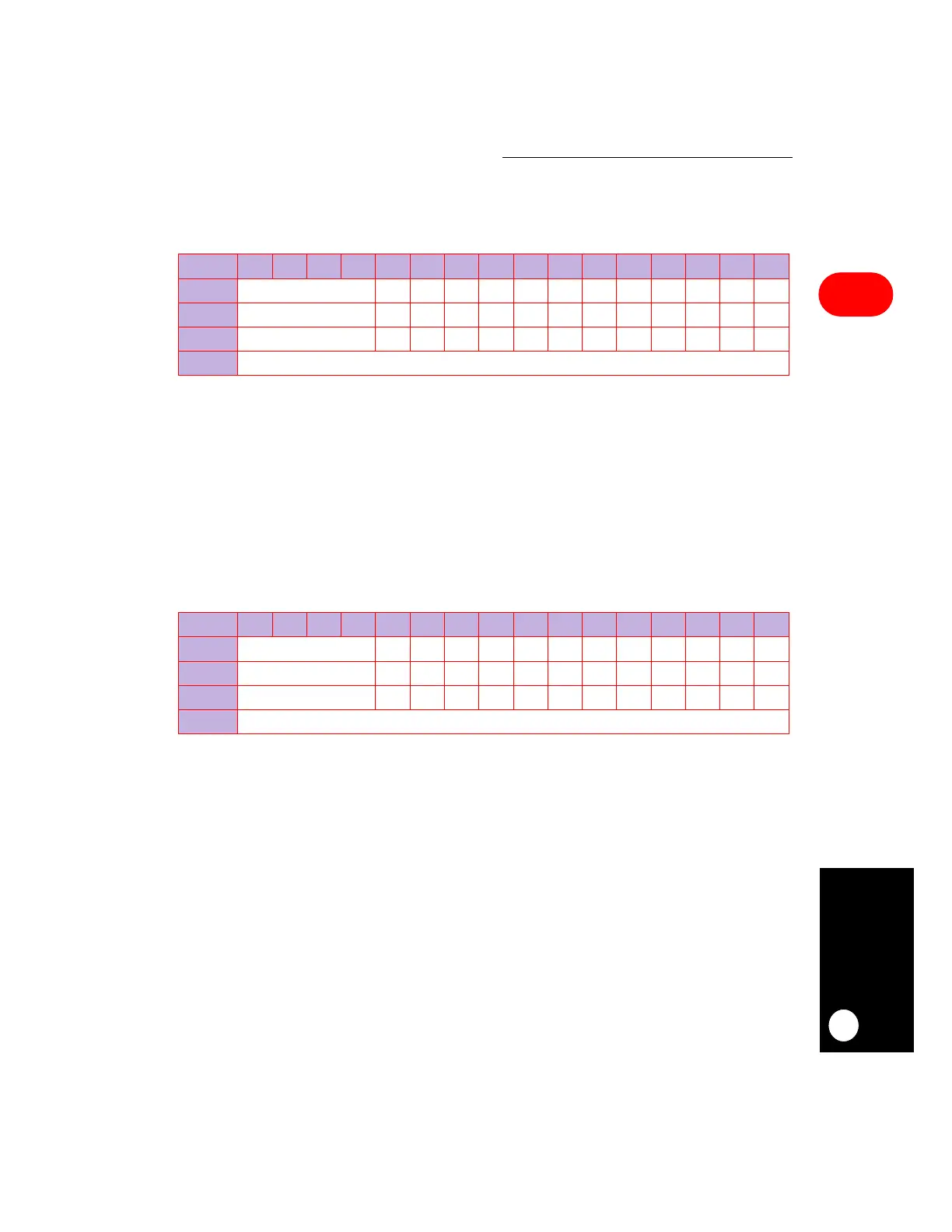
PADIR
BIT 0 1 2 3 4 5 6 7 8 9 10 11 12 13 14 15
FIELD RESERVED DR4 DR5 DR6 DR7 DR8 DR9 DR10 DR11 DR12 DR13 DR14 DR15
RESET 0 000000000000
R/W R/W R/W R/W R/W R/W R/W R/W R/W R/W R/W R/W R/W R/W
ADDR (IMMR & 0xFFFF0000) + 0x950
PAPAR
BIT 0 1 2 3 4 5 6 7 8 9 10 11 12 13 14 15
FIELD RESERVED DD4 DD5 DD6 DD7 DD8 DD9 DD10 DD11 DD12 DD13 DD14 DD15
RESET 0 000000000000
R/W R/W R/W R/W R/W R/W R/W R/W R/W R/W R/W R/W R/W R/W
ADDR (IMMR & 0xFFFF0000) + 0x952