Communication Processor Module
MOTOROLA MPC823e REFERENCE MANUAL 16-483
PORTS
COMMUNICATION
16
PROCESSOR MODULE
PA7 can be configured as a general-purpose I/O pin, but not an open-drain pin. If the
corresponding PADIR bit is a zero, it can also be the CLK1 pin, the TIN1 pin, the L1RCLKA
pin, or all three at once. There is nothing to select other than these three inputs in port A
because the connections are made separately in the serial interface and timer mode
registers. If the PADIR bit is a 1, this pin can also be the BRGO1 pin. If the PA7 pin is a
general-purpose I/O pin, then the input to the on-chip peripheral is internally connected to
BRG01. Refer to Section 16.7 The Serial Interface with Time-Slot Assigner for more
details about using the CLK1 and L1RCLKA pins.
PA4 can be configured as a general-purpose I/O pin, but not an open-drain pin. If the PADIR
bit is zero, PA4 can also be the CLK4 pin, TIN4 pin, L1TCLKB pin or all three at once. If the
PADIR bit is a 1, PA4 can be the TOUT2
pin. If the PA4 pin is a general-purpose I/O pin,
then the input to the on-chip CLK4 function is grounded. Refer to Section 16.7 The Serial
Interface with Time-Slot Assigner for more details.
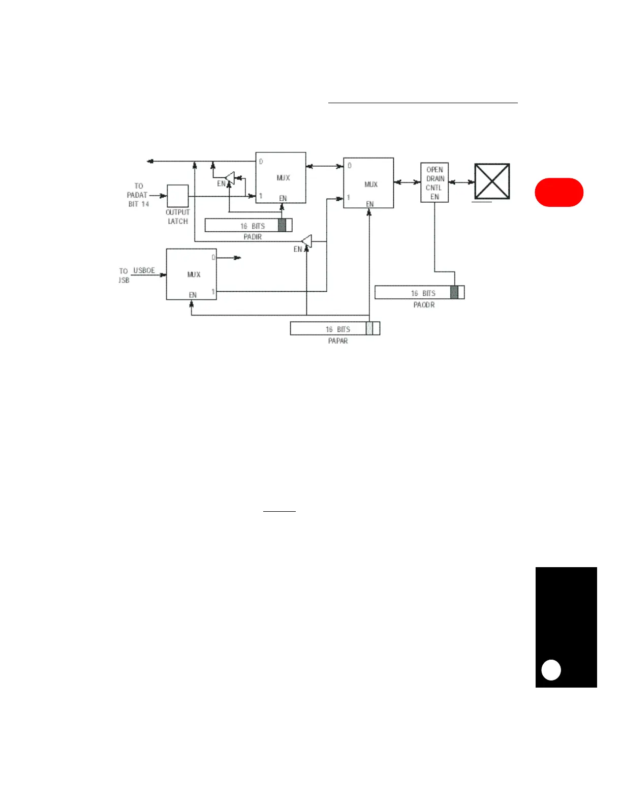
Figure 16-134. Parallel Block Diagram For PA14
USBOE/PA14
PIN
USBOE/PA14
PIN