Communication Processor Module
16-484 MPC823e REFERENCE MANUAL MOTOROLA
PORTS
COMMUNICATION
16
PROCESSOR MODULE
16.14.5 Port B Pin Functionality
All port B pins can be open-drain and are independently configured as general-purpose
I/O pins if the corresponding bit in the PBPAR is cleared. They are configured as dedicated
on-chip peripheral pins if the corresponding PBPAR bit is set. When configured as a
general-purpose I/O pin, the signal direction of that pin is determined by the corresponding
control bit in the PBDIR. The port B pin is configured as an input if the corresponding PBDIR
bit is cleared and as an output if the corresponding PBDIR bit is set. All PBPAR bits and
PBDIR bits are cleared by total system reset, which configures all port B pins as
general-purpose input pins. Refer to Table 16-42 for a description of all port B pin options.
If a port B pin is used as a general-purpose I/O pin, it can be accessed with the PBDAT
where data is stored in an output latch. If a port B pin is configured as an output, the output
latch data is gated onto the port pin. When PBDAT is read, the port pin itself is read. If a port
B pin is configured as an input, data written to PBDAT is still stored in the output latch, but
is prevented from reaching the port pin. When PBDAT is read, the state of the port pin is
read. Many of the port B pins have more than one function, including on-chip peripheral
functions for SPI, I
2
C, SMC1, SMC2, SCC3, TDM, and LCD. PB27 and PB26 are unusual
in that their on-chip peripheral functions (BRGO2 and BRGO1) are also used in port A. This
allows an alternate way to output the BRGO pins if other functions are used. PB18 and PB16
are also unusual in that their on-chip peripheral functions (RTS2 and L1RQA) are used in
port C, which is an alternate location to output these pins if using other functions on port C.
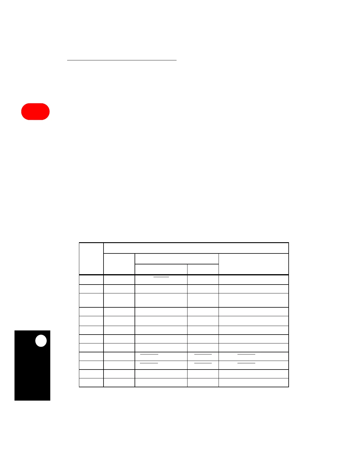
Table 16-42. Port B Pin Assignment
SIGNAL PIN FUNCTION
PBPAR = 0 PBPAR = 1 INPUT TO ON-CHIP
PERIPHERALS
PBDIR = 0 PBDIR = 1
PB31 PORT B31 SPISEL LCD_A SPISEL=V
DD
PB30 PORT B30 TXD3 SPICLK SPICLK = GND
PB29 PORT B29 RXD3 SPIMOSI
SPIMOSI=V
DD
;TXD3 = PB24
(RXD3)
PB28 PORT B28 BRGO3 SPIMISO SPIMISO = SPIMOSI
PB27 PORT B27 BRGO1 I2CSDA I2CSDA= V
DD
PB26 PORT B26 BRGO2 I2CSCL I2CSCL = GND
PB25 PORT B25 SMTXD1 TXD3 —
PB24 PORT B24 SMRXD1/L1RXDB RXD3 SMRXD1 = VCC;RXD3 = GND
PB23 PORT B23 SMSYN1/L1TSYNCB SDACK1 SMSYN1 = GND
PB22 PORT B22 SMSYN2/L1RSYNCB SDACK2 SMSYN2 = GND
PB19 PORT B19 L1ST1 LCD_B —
PB18 PORT B18 L1ST2 RTS2 —