© Koninklijke Philips Electronics N.V. 2006. All rights reserved.
User manual Rev. 01 — 12 January 2006 172
Philips Semiconductors
UM10161
Volume 1 Chapter 13: SSP
CPHA bit is logic zero. Therefore the master device must raise the SSEL pin of the slave
device between each data transfer to enable the serial peripheral data write. On
completion of the continuous transfer, the SSEL pin is returned to its idle state one SCK
period after the last bit has been captured.
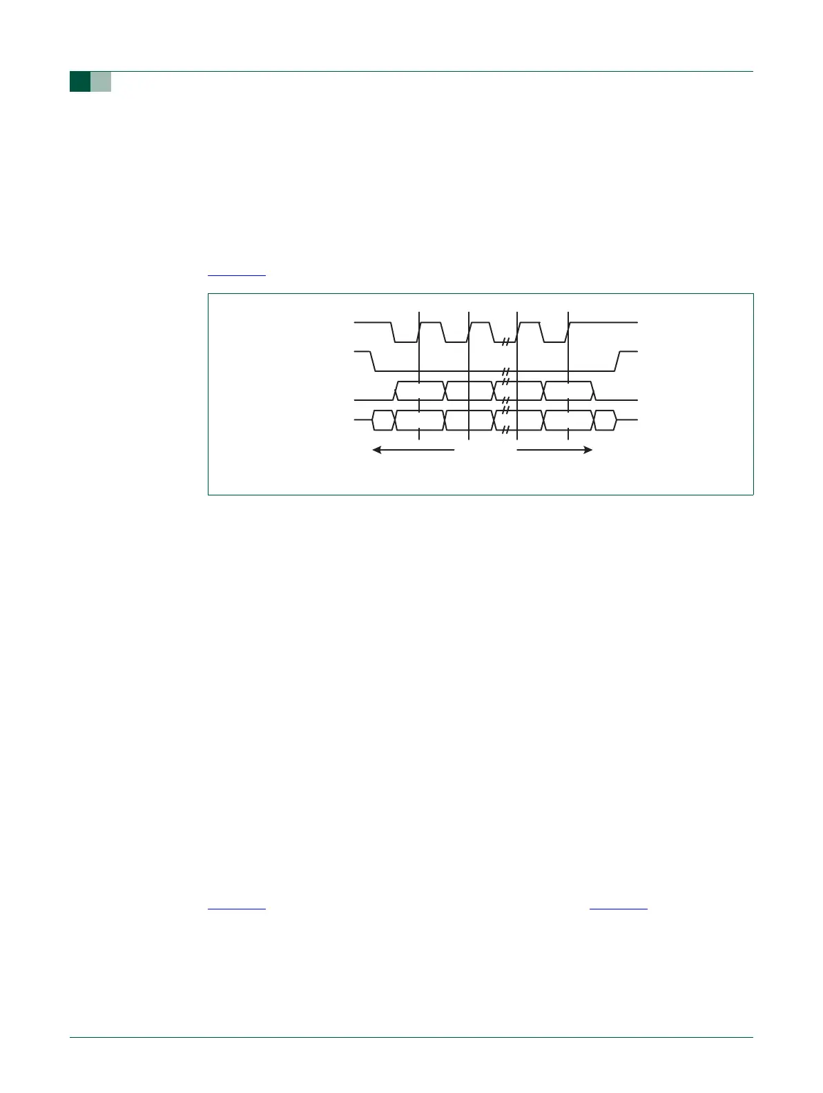
13.3.7 SPI format with CPOL = 1,CPHA = 1
The transfer signal sequence for SPI format with CPOL = 1, CPHA = 1 is shown in
Figure 45
, which covers both single and continuous transfers.
In this configuration, during idle periods:
• The CLK signal is forced HIGH
• SSEL is forced HIGH
• The transmit MOSI/MISO pad is in high impedance
If the SSP is enabled and there is valid data within the transmit FIFO, the start of
transmission is signified by the SSEL master signal being driven LOW. Master’s MOSI is
enabled. After a further one half SCK period, both master and slave data are enabled onto
their respective transmission lines. At the same time, the SCK is enabled with a falling
edge transition. Data is then captured on the rising edges and propagated on the falling
edges of the SCK signal.
After all bits have been transferred, in the case of a single word transmission, the SSEL
line is returned to its idle HIGH state one SCK period after the last bit has been captured.
For continuous back-to-back transmissions, the SSEL pins remains in its active LOW
state, until the final bit of the last word has been captured, and then returns to its idle state
as described above. In general, for continuous back-to-back transfers the SSEL pin is held
LOW between successive data words and termination is the same as that of the single
word transfer.
13.3.8 Semiconductor Microwire frame format
Figure 46 shows the Microwire frame format for a single frame. Figure 47 shows the same
format when back-to-back frames are transmitted.
Fig 45. Motorola SPI frame format with CPOL = 1 and CPHA = 1 (single transfer)
SCK
SSEL
MOSI
Q
4 to 16 bits
MISO
Q MSB
MSB LSB
LSB