© Koninklijke Philips Electronics N.V. 2006. All rights reserved.
User manual Rev. 01 — 12 January 2006 61
Philips Semiconductors
UM10161
Volume 1 Chapter 6: Pin configuration
6.2 Pin description for LPC2101/02/03
Pin description for LPC2101/02/03 and a brief explanation of corresponding functions are
shown in the following table.
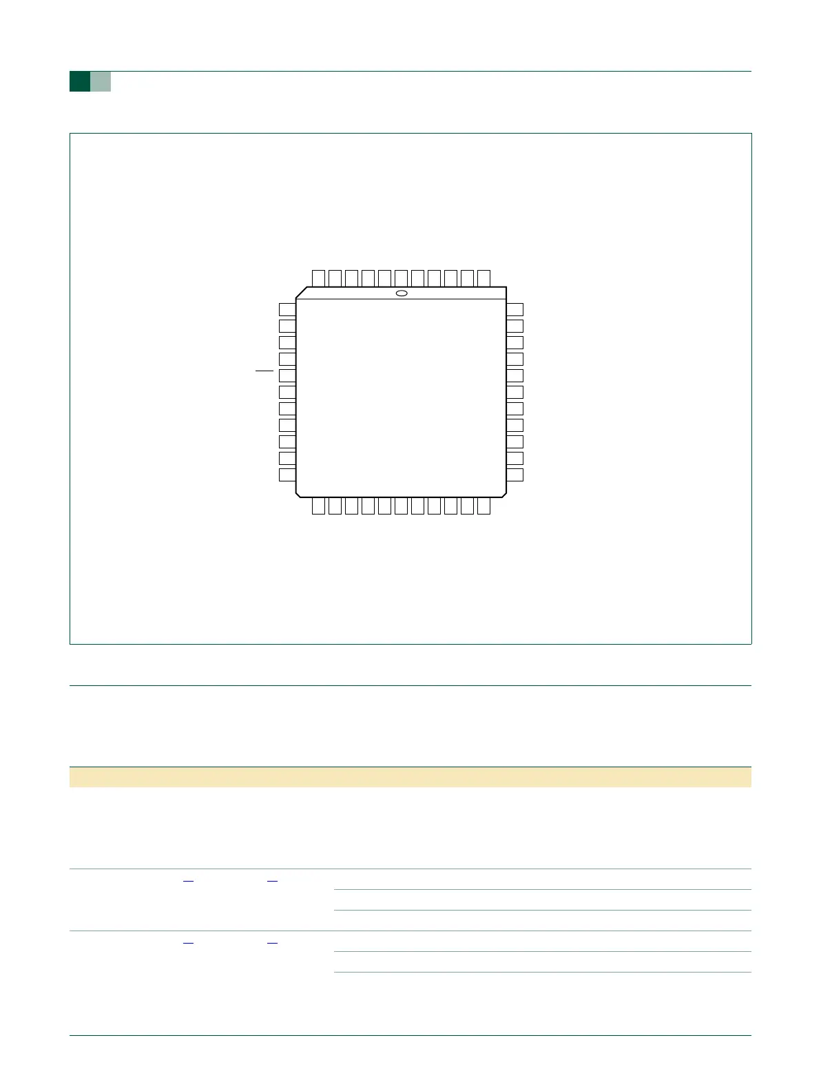
Fig 15. PLCC44 pin configuration
LPC2101/2102/2103
002aab920
7
8
9
10
11
12
13
14
15
16
17
39
38
37
36
35
34
33
32
31
30
29
18
19
20
21
22
23
24
25
26
27
28
6
5
4
3
2
1
44
43
42
41
40
P0.27/TRST/CAP2.0
V
SS
P0.28/TMS/CAP2.1
V
DDA
P0.29/TCK/CAP2.2
P0.13/DTR1/MAT1.1
X1
V
DD(3V3)
X2
P0.25/AD0.6
P0.0/TXD0/MAT3.1
P0.12/DSR1/MAT1.0/AD0.5
P0.1/RXD0/MAT3.2
P0.11/CTS1/CAP1.1/AD0.4
P0.30/TDI/MAT3.3
P0.10/RTS1/CAP1.0/AD0.3
P0.31/TDO
P0.24/AD0.2
P0.2/SCL0/CAP0.0
P0.23/AD0.1
V
SS
P0.22/AD0.0
RTXC1
V
SS
P0.3/SDA0/MAT0.0
RST
P0.4/SCK0/CAP0.1
V
DD(1V8)
P0.5/MISO0/MAT0.1
P0.21/SSEL1/MAT3.0
P0.6/MOSI0/CAP0.2
P0.20/MAT1.3/MOSI1
RTXC2
P0.19/MAT1.2/MISO1
DBGSEL
P0.18/CAP1.3/SDA1
P0.7/SSEL0/MAT2.0
P0.17/CAP1.2/SCL1
P0.8/TXD1/MAT2.1
P0.16/EINT0/MAT0.2
P0.9/RXD1/MAT2.2
P0.15/RI1/EINT2
V
SSA
P0.14/DCD1/SCK1/EINT1
Table 58: Pin description
Symbol LQFP48 PLCC44 Type Description
P0.0 to P0.31 I/O Port 0: Port 0 is a 32-bit I/O port with individual direction
controls for each bit. A total of 31 pins of the Port 0 can be
used as general purpose bidirectional digital I/Os while P0.31
is an output only pin. The operation of port 0 pins depends
upon the pin function selected via the pin connect block.
P0.0/TXD0/
MAT3.1
13
[1]
18
[1]
I/O P0.0 — General purpose Input/output digital pin (GPIO).
O TXD0 — Transmitter output for UART0.
O MAT3.1 — PWM output 1 for Timer 3.
P0.1/RXD0/
MAT3.2
14
[2]
19
[2]
I/O P0.1 — General purpose Input/output digital pin (GPIO).
I RXD0 — Receiver input for UART0.
O MAT3.2 — PWM output 2 for Timer 3.