© Koninklijke Philips Electronics N.V. 2006. All rights reserved.
User manual Rev. 01 — 12 January 2006 40
Philips Semiconductors
UM10161
Volume 1 Chapter 4: MAM Module
4.3 MAM blocks
The Memory Accelerator Module is divided into several functional blocks:
• A Flash Address Latch and an incrementor function to form prefetch addresses
• A 128-bit Prefetch Buffer and an associated Address latch and comparator
• A 128-bit Branch Trail Buffer and an associated Address latch and comparator
• A 128-bit Data Buffer and an associated Address latch and comparator
• Control logic
• Wait logic
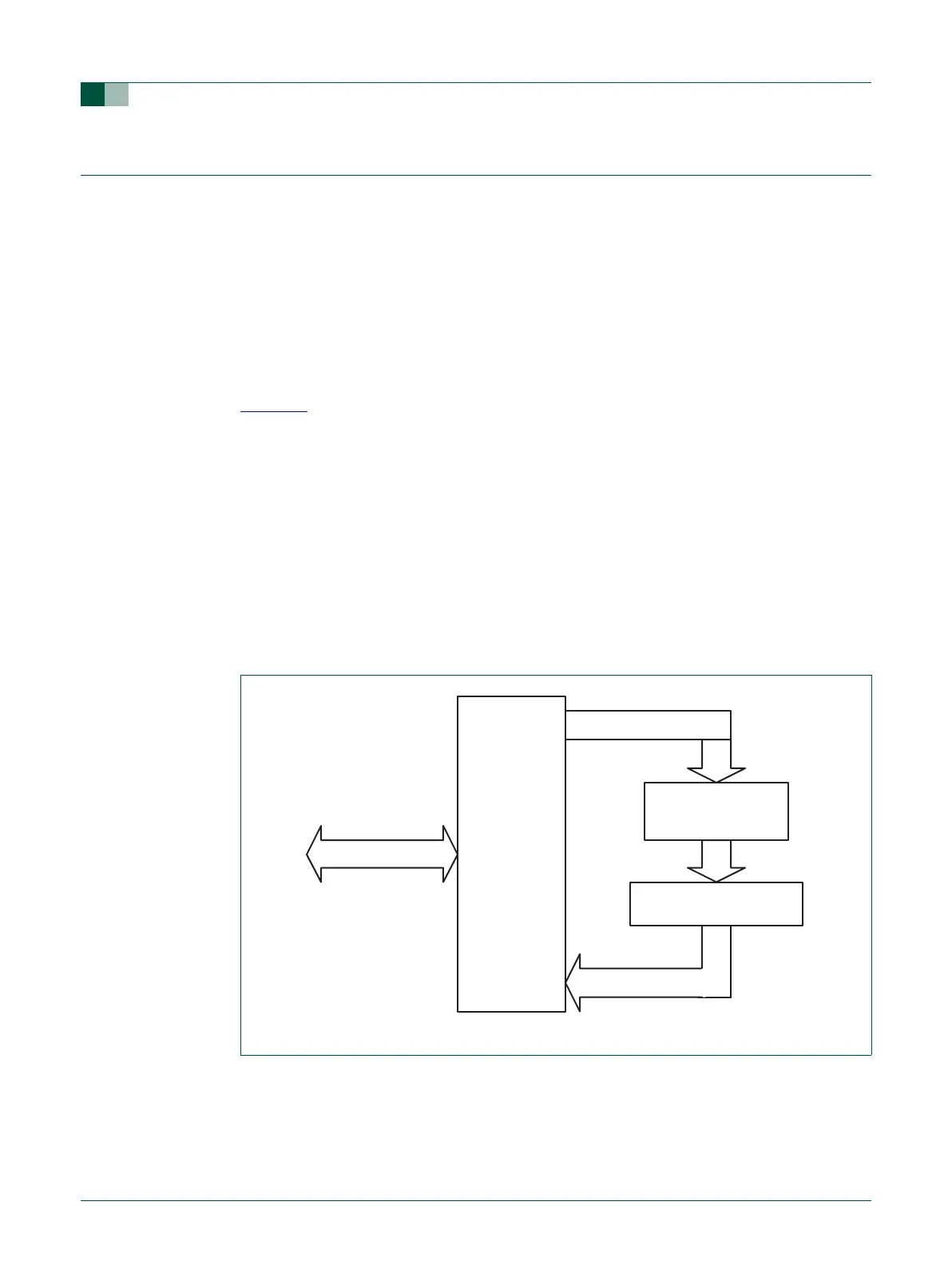
Figure 12
shows a simplified block diagram of the Memory Accelerator Module data paths.
In the following descriptions, the term “fetch” applies to an explicit Flash read request from
the ARM. “Pre-fetch” is used to denote a Flash read of instructions beyond the current
processor fetch address.
4.3.1 Flash memory bank
There is one bank of Flash memory with the LPC2101/02/03 MAM.
Flash programming operations are not controlled by the MAM but are handled as a
separate function. A “boot block” sector contains flash programming algorithms that may
be called as part of the application program and a loader that may be run to allow serial
programming of the flash memory.
4.3.2 Instruction latches and data latches
Code and Data accesses are treated separately by the Memory Accelerator Module.
There is a 128-bit Latch, a 15-bit Address
Fig 12. Simplified block diagram of the Memory Accelerator Module (MAM)
BUS
INTERFACE
BUFFERS
MEMORY ADDRESS
ARM LOCAL BUS
FLASH MEMORY BANK