© Koninklijke Philips Electronics N.V. 2006. All rights reserved.
User manual Rev. 01 — 12 January 2006 253
Philips Semiconductors
UM10161
Volume 1 Chapter 20: EmbeddedICE
allowing an interval between the release of the external reset and the release of the internal
reset during which RTCK may be driven by an external signal if necessary.
This procedure establishes the P0.27 - P0.31 pins as the JTAG Test/Debug interface. Pin
connect block settings have no affect on P0.27 - P0.31 pins if they are initialized as JTAG
pins.
For the effect of hardware override related to DBGSEL and RTCK see Ta ble 5 8
in Section
6.2 “Pin description for LPC2101/02/03” on page 61.
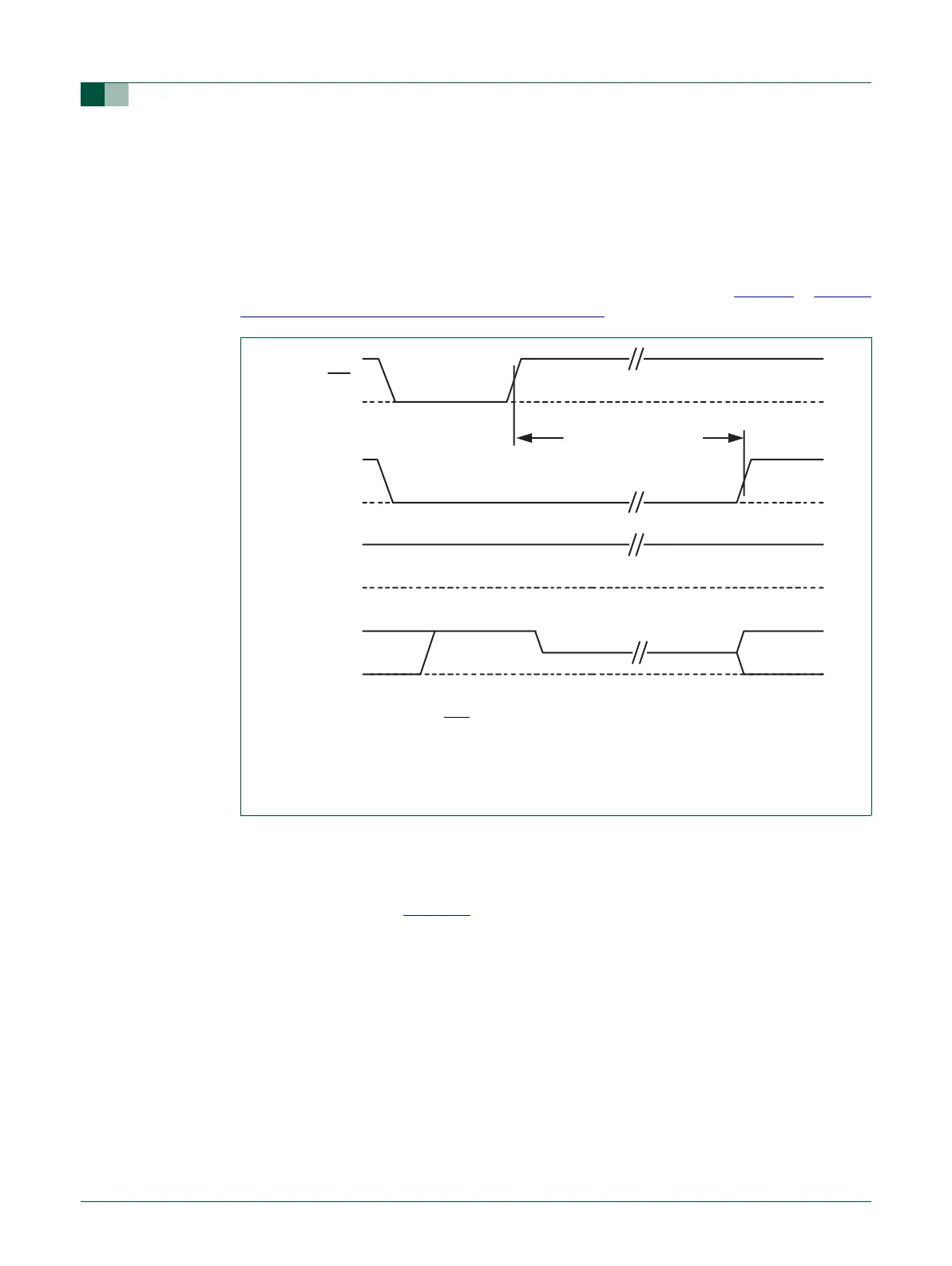
20.8.2 JTAG pin selection
The Primary JTAG port can be selected for debugging only when DBGSEL and RTCK pins
are HIGH at reset (see Figure 66
). If at least one of the DBGSEL or RTCK lines is LOW at
reset, JTAG will not be enabled and can not be used for later debugging.
(1) DBGSEL must be HIGH.
(2) RTCK must be HIGH as RST
is released. An internal pull-up will cause RTCK to be HIGH if it
is not pulled LOW externally.
(3) The RTCK output driver will be turned on when the internal chip reset is released by the
wake-up timer.
Fig 66. Waveforms for debug mode using the primary JTAG pins.
RST
DBGSEL
1
RTCK
2,3
wake-up timer count time
internal reset