© Koninklijke Philips Electronics N.V. 2006. All rights reserved.
User manual Rev. 01 — 12 January 2006 67
Philips Semiconductors
UM10161
Volume 1 Chapter 7: Pin connect block
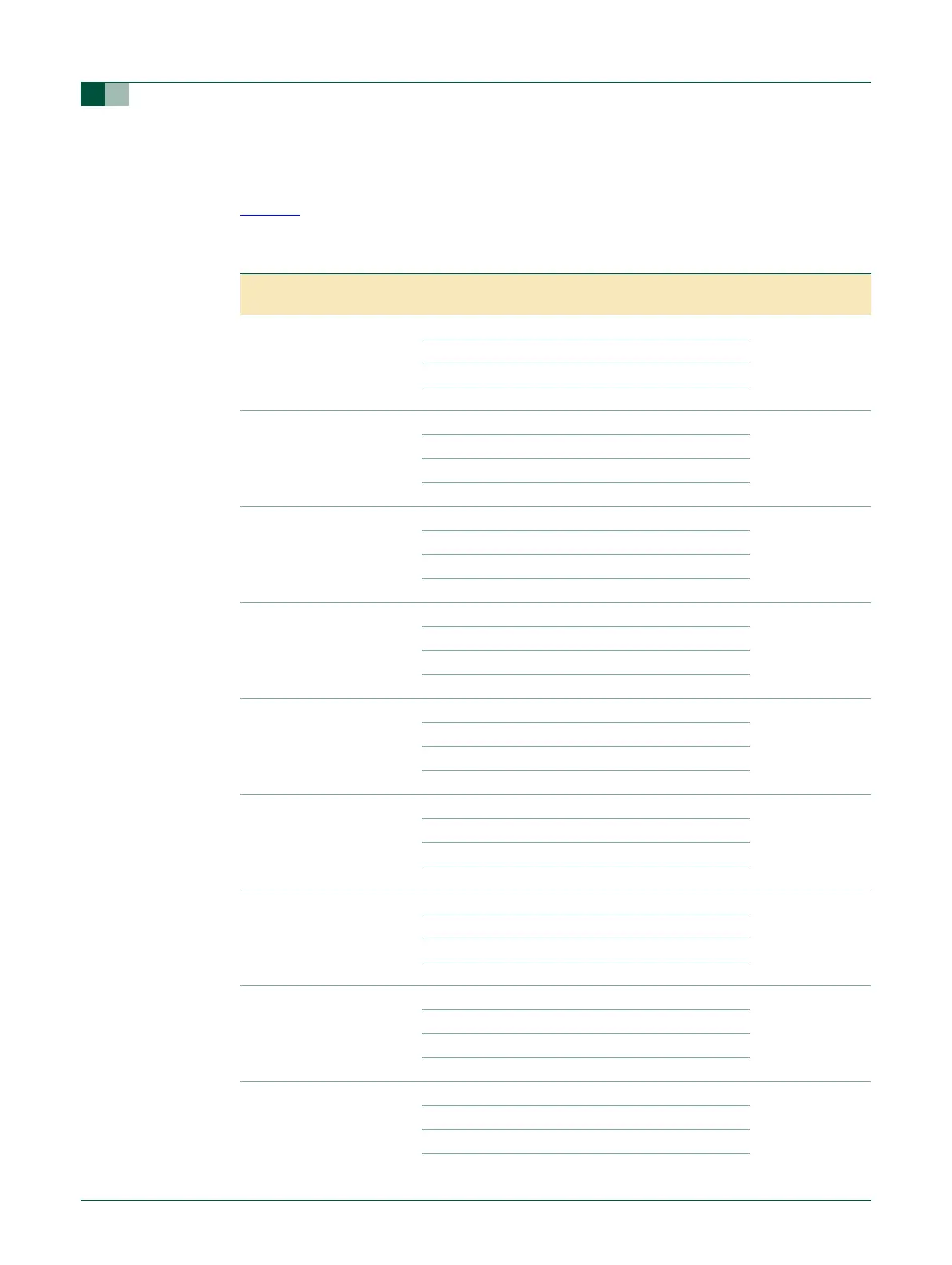
7.4.1 Pin function Select register 0 (PINSEL0 - 0xE002 C000)
The PINSEL0 register controls the functions of the pins as per the settings listed in
Tabl e 6 2
. The direction control bit in the IO0DIR register is effective only when the GPIO
function is selected for a pin. For other functions, direction is controlled automatically.
Table 60: Pin function select register 0 (PINSEL0 - 0xE002 C000)
PINSEL0 Pin name Value Function Value after
reset
1:0 P0.0 0 0 GPIO Port 0.0 0
01TXD0 (UART0)
1 0 MAT3.1(Timer 3)
11Reserved
3:2 P0.1 0 0 GPIO Port 0.1 0
01RXD0 (UART0)
1 0 MAT3.2 (Timer 3)
11Reserved
5:4 P0.2 0 0 GPIO Port 0.2 0
0 1 SCL0 (I
2
C0)
1 0 CAP0.0 (Timer 0)
11Reserved
7:6 P0.3 0 0 GPIO Port 0.3 0
01SDA0 (I
2
C0)
1 0 MAT0.0 (Timer 0)
11Reserved
9:8 P0.4 0 0 GPIO Port 0.4 0
0 1 SCK0 (SPI0)
1 0 CAP0.1 (Timer 0)
11Reserved
11:10 P0.5 0 0 GPIO Port 0.5 0
0 1 MISO0 (SPI0)
1 0 MAT0.1 (Timer 0)
11Reserved
13:12 P0.6 0 0 GPIO Port 0.6 0
0 1 MOSI0 (SPI0)
1 0 CAP0.2 (Timer 0)
11Reserved
15:14 P0.7 0 0 GPIO Port 0.7 0
0 1 SSEL0 (SPI0)
1 0 MAT2.0 (Timer 2)
11Reserved
17:16 P0.8 0 0 GPIO Port 0.8 0
01TXD1 (UART1)
1 0 MAT2.1 (Timer 2)
11Reserved