S3F84B8_UM_REV 1.00 1 OVERVIEW OF S3F84B8 MICROCONTROLLER
1-12
Figure 1-7 shows the Pin Circuit Type 1-3 (P0.3, P0.4, P0.6) in S3F84B8.
I/O
Output
Disable
Data
Pin Circuit
Type 1
Pull-up
Enable
VDD
Pull-up register
(50 kohm typical)
Noise
Filter
Ext.INT
Input
MUX
Pin config bits
Figure 1-7 Pin Circuit Type 1-3 (P0.3, P0.4, P0.6)
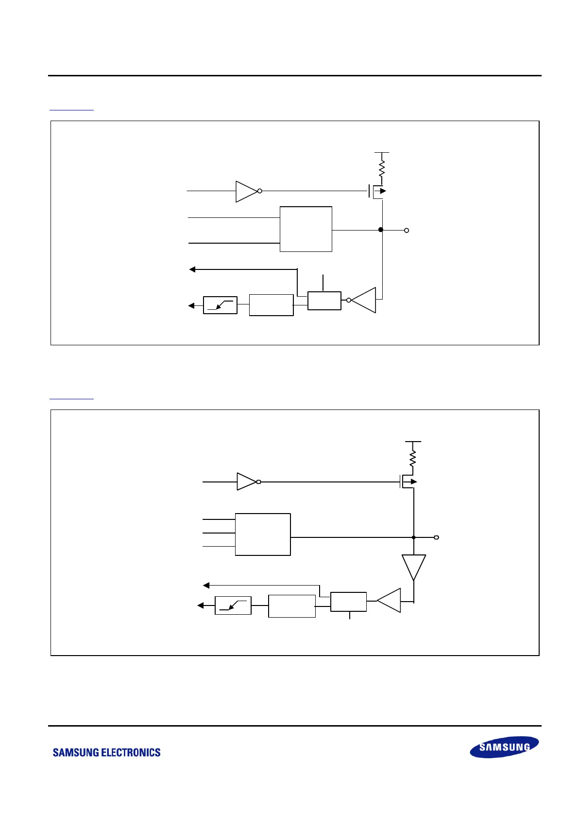
Figure 1-8
shows the Pin Circuit Type 2-1 (P0.5) in S3F84B8.
VDD
I/O
Output DIsable
(input mode)
Data
Pull-up register
(50 kohm typical)
Pull-up
enable
Pin Circuit
Type 2
Open drain
enable
Noise
Filter
Ext.INT
MUX
Pin configure bits
Input
Figure 1-8 Pin Circuit Type 2-1 (P0.5)
 Loading...