OSSD 1.A
V
t
OSSD 1.B
V
t
t
S
t
S
t
S
t
S
t
S
t
S
t
S
t
S
t
S
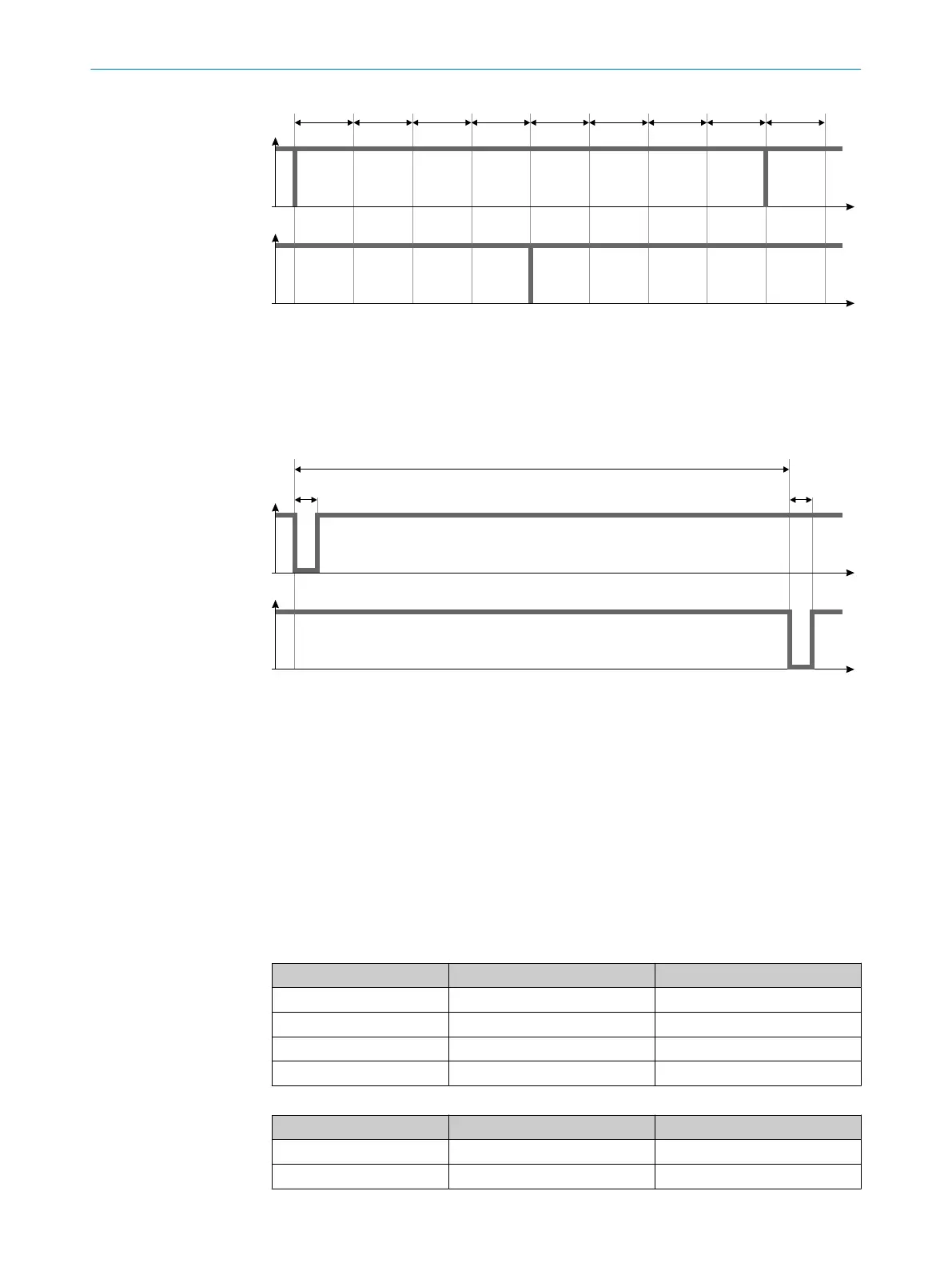
Figure 73: Switch-off tests
t
S
Scan cycle time
•
Se
tting “30 ms”: t
S
= 30 ms
•
Setting “40 ms”: t
S
= 40 ms
•
Setting “50 ms”: t
S
= 50 ms
OSSD 1.A
V
t
OSSD 1.B
V
t
≤ 300
µs
≤ 300
µs
S
4 × t
Figure 74: Duration and time offset for the switch-off tests in an OSSD pair
t
S
Scan cycle time
•
Se
tting “30 ms”: t
S
= 30 ms
•
Setting “40 ms”: t
S
= 40 ms
•
Setting “50 ms”: t
S
= 50 ms
13.6 Sensing range
Protective field range
T
he effective protective field range depends on the variant, on the set scan cycle time
and on the set object resolution.
Table 30: Protective field range (devices with a max. protective field range of 4.0 m)
Resolution Scan cycle time 40 ms Scan cycle time 30 ms
≥ 70 mm 4.00 m 4.00 m
50 mm 3.50 m 3.00 m
40 mm 3.00 m 2.30 m
30 mm 2.30 m 1.70 m
Table 31: Protective field range (devices with a max. protective field range of 5.5 m)
Resolution Scan cycle time 40 ms Scan cycle time 30 ms
≥ 70 mm 5.50 m 4.00 m
50 mm 3.50 m 3.00 m
TECHNICAL DATA 13
8017784/1ELL/2022-01-21 | SICK O P E R A T I N G I N S T R U C T I O N S | microScan3 Core I/O AIDA
133
Subject to change without notice

 Loading...