Memory Controller
MOTOROLA MPC823e REFERENCE MANUAL 15-29
MEMORY CONTROLLER
15
Next, the banks selected by the general-purpose chip-select machine support an option to
output the CSx
signal at different timings with respect to the external address bus. CSx can
be output in any of the following configurations:
• Simultaneous with the external address
• One quarter of a clock later
• One half of a clock later
This all depends, of course, on the value in the ACS field of the ORx register, plus an
additional cycle if the TRLX bit is set. The general-purpose chip-select machine allows you
to connect to devices that have long disconnect times on data by delaying new bus
transactions addressing other memory banks for additional clock cycles. Finally, the banks
selected to operate with the general-purpose chip-select machine support termination of an
external cycle by sensing the TA
signal asserted by the addressed external slave. Refer
back to Table 15-2 for more information.
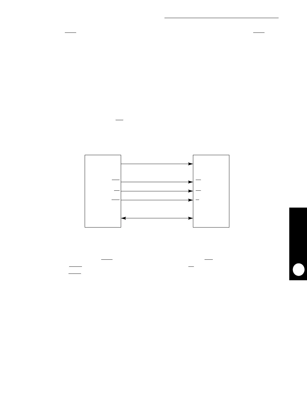
Figure 15-5 illustrates a basic connection between the MPC823e and a “static” memory
device. In this case, the CSx
signal is connected directly to the CE signal of the memory
device. The WEx
signals are connected to the respective W signal of the memory device in
which each WEx
signal corresponds to a different data byte.
MPC823e MEMORY
Figure 15-5. GPCM Memory Device Interface
ADDRESS
CE
OE
W
DATA
ADDRESS
CS
x
OE
WEx
DATA
 Loading...

