Memory Controller
15-30 MPC823e REFERENCE MANUAL MOTOROLA
MEMORY CONTROLLER
15
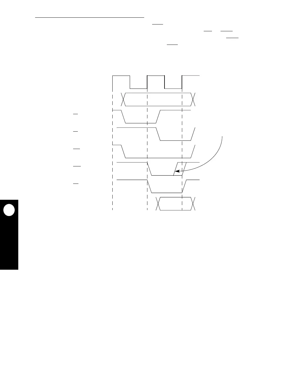
As illustrated in Figure 15-6, the timing of the CSx signal is the same as the timing of the
address lines. The strobes for the transaction are supplied by the OE
or WEx signals,
depending on the transaction direction (read or write). The negation of the WEx
signal is
controlled by the CSNT bit of the ORx register. The CSx
signal is generated when the ACS
field in the corresponding ORx register is set to ‘00’.
Figure 15-6. GPCM Memory Device Basic Timing
(ACS = 00, CSNT = 1, and TRLX = 0)
CLOCK
ADDRESS
CS
x
WEx
OE
DATA
TS
TA
CSNT = 1
 Loading...

