Communication Processor Module
16-252 MPC823e REFERENCE MANUAL MOTOROLA
COMMUNICATION
16
SCCs
A bit is cleared by writing a 1 (writing a zero has no effect) and more than one bit can be
cleared at a time. Also, all unmasked bits must be cleared before the communication
processor module clears the internal interrupt request. This register is cleared at reset and
can be read at any time.
Bits 0–2 and 9–10—Reserved
These bits are reserved and must be set to 0.
GLR—Glitch on RX
If set, this bit indicates that a serial communication controller has detected a clock glitch on
the receive clock.
GLT—Glitch on TX
If set, this bit indicates that a serial communication controller has detected a clock glitch on
the transmit clock.
DCC—DPLL Carrier-Sense Changed
This bit indicates that the carrier-sense status generated by the DPLL has changed state.
Its real-time status can be found in the SCCS–HDLC register. This is not the CDx
pin status
that is reported in port C and it is only valid when the DPLL is used.
FLG—Flag Status
This bit indicates that the SCCx HDLC controller has stopped or started receiving HDLC
flags. Its real-time status can be obtained in the SCCS–HDLC register.
IDL—Idle Sequence Status Changed
This bit indicates that a change has occurred in the status of the serial line on the HDLC line.
The real-time status of the line can be read in the SCCS–HDLC register.
GRA—Graceful Stop Complete
This bit indicates that a graceful stop, which was initiated by the GRACEFUL STOP
TRANSMIT command, has completed. This bit is set as soon as the transmitter finishes
transmitting any frame that was in progress when the command was issued. It is set
immediately if no frame was in progress when the command was issued.
TXE—TX Error
This bit indicates that an error has occurred on the transmitter channel.
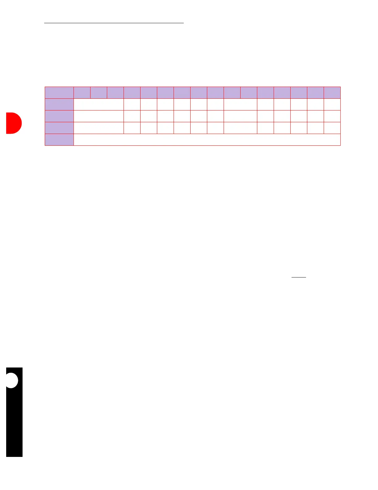
SCCE–HDLC
BIT 0 1 2 3 4 5 6 7 8 9 10 11 12 13 14 15
FIELD RESERVED GLR GLT DCC FLG IDL GRA RESERVED TXE RXF BSY TXB RXB
RESET 0 000000 0 00000
R/W R/W R/W R/W R/W R/W R/W R/W R/W R/W R/W R/W R/W R/W
ADDR (IMMR & 0xFFFF0000) + 0xA30