© Koninklijke Philips Electronics N.V. 2006. All rights reserved.
User manual Rev. 01 — 12 January 2006 158
Philips Semiconductors
UM10161
Volume 1 Chapter 12: SPI
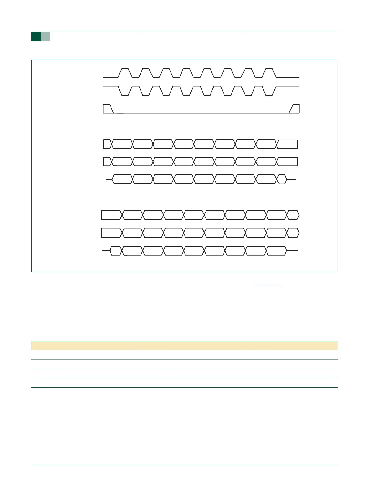
The data and clock phase relationships are summarized in Tabl e 138. This table
summarizes the following for each setting of CPOL and CPHA.
• When the first data bit is driven
• When all other data bits are driven
• When data is sampled
The definition of when an 8 bit transfer starts and stops is dependent on whether a device
is a master or a slave, and the setting of the CPHA variable.
When a device is a master, the start of a transfer is indicated by the master having a byte
of data that is ready to be transmitted. At this point, the master can activate the clock, and
begin the transfer. The transfer ends when the last clock cycle of the transfer is complete.
Fig 39. SPI data transfer format (CPHA = 0 and CPHA = 1)
MISO (CPHA = 1)
MOSI (CPHA = 1)
Cycle # CPHA = 1
CPHA = 1
MISO (CPHA = 0)
MOSI (CPHA = 0)
Cycle # CPHA = 0
CPHA = 0
SSEL
SCK (CPOL = 1)
SCK (CPOL = 0)
123 87654
BIT 1 BIT 2 BIT 3 BIT 8BIT 7BIT 6BIT 5BIT 4
BIT 1 BIT 2 BIT 3 BIT 8BIT 7BIT 6BIT 5BIT 4
123 87654
BIT 1 BIT 2 BIT 3 BIT 8BIT 7BIT 6BIT 5BIT 4
BIT 1 BIT 2 BIT 3 BIT 8BIT 7BIT 6BIT 5BIT 4
Table 138: SPI data to clock phase relationship
CPOL and CPHA settings First data driven Other data driven Data sampled
CPOL = 0, CPHA = 0 Prior to first SCK rising edge SCK falling edge SCK rising edge
CPOL = 0, CPHA = 1 First SCK rising edge SCK rising edge SCK falling edge
CPOL = 1, CPHA = 0 Prior to first SCK falling edge SCK rising edge SCK falling edge
CPOL = 1, CPHA = 1 First SCK falling edge SCK falling edge SCK rising edge