© Koninklijke Philips Electronics N.V. 2006. All rights reserved.
User manual Rev. 01 — 12 January 2006 17
Philips Semiconductors
UM10161
Volume 1 Chapter 3: System control block
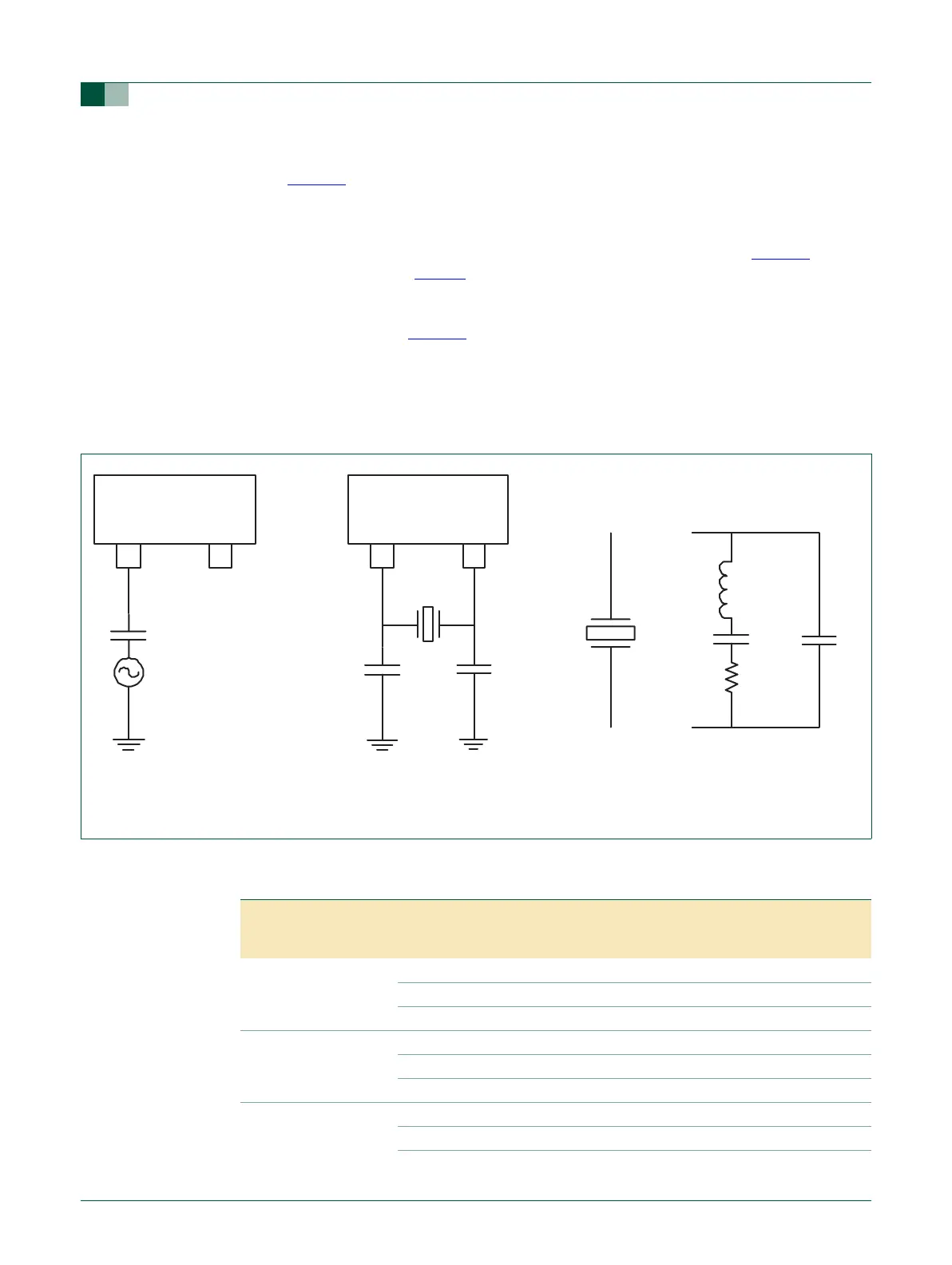
In slave mode the input clock signal should be coupled by means of a capacitor of 100 pF
(C
C
in Figure 6, drawing a), with an amplitude of at least 200 mVrms. The X2 pin in this
configuration can be left not connected. If slave mode is selected, the F
OSC
signal of 50-50
duty cycle can range from 1 MHz to 50 MHz.
External components and models used in oscillation mode are shown in Figure 6
,
drawings b and c, and in Tabl e 7
. Since the feedback resistance is integrated on chip, only
a crystal and the capacitances C
X1
and C
X2
need to be connected externally in case of
fundamental mode oscillation (the fundamental frequency is represented by L, C
L
and
R
S
). Capacitance C
P
in Figure 6, drawing c, represents the parallel package capacitance
and should not be larger than 7 pF. Parameters F
C
, C
L
, R
S
and C
P
are supplied by the
crystal manufacturer.
Choosing an oscillation mode as an on-board oscillator mode of operation limits F
OSC
clock selection to 1 MHz to 30 MHz.
Fig 6. Oscillator modes and models: a) slave mode of operation, b) oscillation mode of operation, c) external
crystal model used for C
X1
/
X2
evaluation
LPC2101/02/03 LPC2101/02/03
X1X1 X2X2
Clock
C
C
C
X1
C
X2
C
L
C
P
L
R
S
< = >
a) b) c)
Xtal
Table 7: Recommended values for C
X1/X2
in oscillation mode (crystal and external
components parameters)
Fundamental
oscillation frequency
F
OSC
Crystal load
capacitance C
L
Maximum crystal
series resistance R
S
External load
capacitors C
X1
,
CX2
1 MHz - 5 MHz 10 pF NA NA
20 pF NA NA
30 pF < 300 Ω 58 pF, 58 pF
5 MHz - 10 MHz 10 pF < 300 Ω 18 pF, 18 pF
20 pF < 300 Ω 38 pF, 38 pF
30 pF < 300 Ω 58 pF, 58 pF
10 MHz - 15 MHz 10 pF < 300 Ω 18 pF, 18 pF
20 pF < 220 Ω 38 pF, 38 pF
30 pF < 140 Ω 58 pF, 58 pF