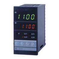
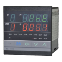
4. BASIC OPERATION
IMR02L04-E3
4-48
PV
F52.
M:S
SV
FIX000RDIAT
Function block 52
(F52.)
PV
KTATB
$
M:S
SV
F52.01R 00000
AT bias
PV
L ATT.R
M:S
SV
F52.07R 00000
AT with learning function
at ramp segment
F52.02: AT differential gap time
F52.03: AT Time signal action
F52.04: AT cycles
F52.05: Output value with AT turned on
F52.06: Output value with AT turned off
Setting parameters from F52.02 to F52.06
Function block 50
(F50.)
PV
F53.
M:S
SV
FIX000VALVE
Function block 53
(F53.)
PV
LCYBR
M:S
SV
F53.01R 00000
Action at feedback
resistance (FBR) input error
PV
LHVAL
M:S
SV
F53.05R 00000
Valve action
in Reset mode
PV
F60.
M:S
SV
FIX000VSCI.1
Function block 60
(F60.)
PV
L CMP1
M:S
SV
F60.01R 00000
Communication 1
protocol
PV
L INT1
M:S
SV
F60.05R 00010
Interval time 1
Function block 71
(F71.)
PV
F61.
M:S
SV
FIX000VSCI.2
Function block 61
(F61.)
PV
SLV.SL
M:S
SV
F61.01R 00000
Slave controlle
PV
L BPS2
M:S
SV
F61.04R 19200
Communication speed 2
PV
SLV.NO
M:S
SV
F61.02R 00000
Number of slave unit
PV
L ADD2
M:S
SV
F61.03R 00000
Device address 2
PV
L ADD1
M:S
SV
F60.02R 00000
Device address 1
PV
L BPS1
M:S
SV
F60.03R 19200
Communication speed 1
PV
L BIT1
M:S
SV
F60.04R198N1
Data bit configuration 1
PV
LCPOS
M:S
SV
F53.02R00ADJ
Feedback adjustment
PV
LCMOT
M:S
SV
F53.03R 00010
Control motor time
PV
LCOLA
%
M:S
SV
F53.04R 0150.0
Integrated output
limiter
PV
H.E R.T M
M:S
SV
F61.05R 00010
Host communication
error judgment time
PV
C.E R.T M
M:S
SV
F61.06R 00010
Intercontrolle
communication
error judgment time
Press the STEP R.SET key to go back to the previous display.
Press the STEP R.SET key while pressing the
key to go
back to the first setting display of the function block.
(P. 4-41)
(P. 4-42)
(P. 4-42)
(P. 4-43)

 Loading...