Operating instructions Chapter 12
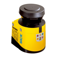
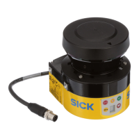
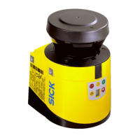
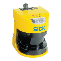
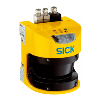
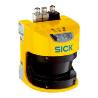
S3000
8009942/WK81/2012-11-28 © SICK AG • Industrial Safety Systems • Germany • All rights reserved 153
Subject to change without notice
Technical specifications
Minimum Typical Maximum
OSSDs
Output signal switching device pair 2 PNP semiconductors, short-circuit
protected
4
0)
, cross-circuit monitored
Safe state in case of an error At least one OSSD is in the LOW state
HIGH switching voltage at 500 mA V
S
– 2.7 V V
S
Switching voltage LOW 0 V 0 V 3.5 V
Source switching current 6 mA 0.2 A 0.5 A
Leakage current
41)
250 µA
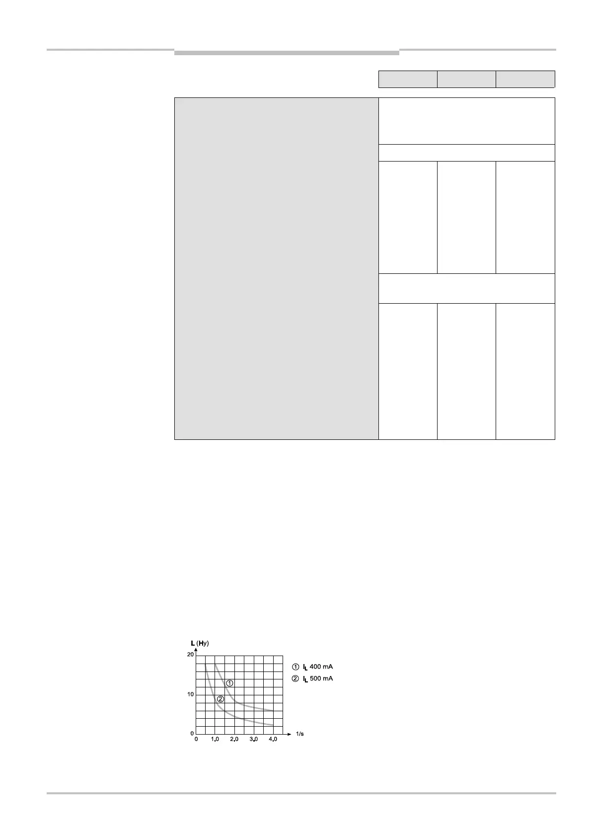
Load inductance
42)
2.2 H
Load capacity 2.2 µF at
50 b
Switching sequence (without switching and
without simultaneous monitoring)
Depending on load inductance
Permissible cable resistance
43)
2.5 b
Test pulse width
44)
230 µs 300 µs
Test frequency
at 0.5° angular resolution
At 0.25° angular resolution
120 ms
240 ms
Power-up delay of the OSSDs from red to
green
120 ms
Time offset on switching the OSSDs between
OSSD2 and OSSD1
1.3 ms 2 ms
40)
Applies to the voltage range between V[0]
S
and 0 V.
41)
In the case of a fault (0 V cable open circuit) maximally the leakage current flows in the OSSD cable. The
downstream controller must detect this status as LOW. A FPLC (fail-safe programmable logic controller) must
be able to identify this status.
42)
The maximum rated load inductance is higher with lower switching sequence.
43)
Make sure to limit the individual line core resistance to the downstream controller to this value to ensure that
a cross-circuit between the outputs is safely detected. (Also note EN 60204<1.)
44)
When active, the outputs are tested cyclically (brief LOW). When selecting the downstream controllers, make
sure that the test signals do not result in deactivation.