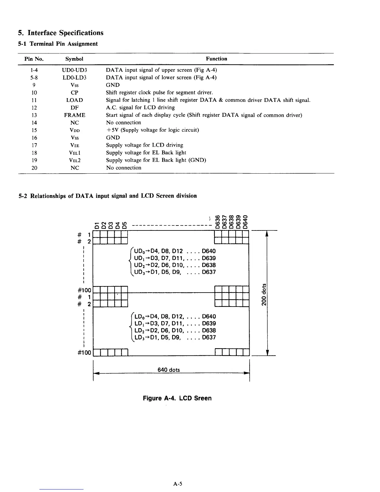
5.
Interface Specifications
5-1
Terminal Pin Assignment
I
#loo
#
1.
#2
Pin
No.
Symbol
Function
1-4
5-8
9
10
11
12
13
14
15
16
17
18
19
20
UDO-UD3
LDO-LD3
vss
CP
LOAD
DF
FRAME
NC
VDD
vss
VEE
VEL
1
NC
VEL2
DATA input signal of upper screen (Fig A-4)
DATA input signal of lower screen (Fig A-4)
GND
Shift register clock pulse for segment driver.
Signal for latching
1
line shift register DATA
&
common driver DATA shift signal.
A.C. signal
for
LCD driving
Start signal
of
each display cycle (Shift register DATA signal of common driver)
No connection
+5V (Supply voltage for logic circuit)
GND
Supply voltage for LCD driving
Supply voltage for EL Back light
Supply voltage for EL Back light (GND)
No connection
5-2
Relationships
of
DATA input signal and
LCD
Screen division
#
#
1
2
.
(Dl-wmo
C3c)Oc)b
-(Vc)bv)
(D(D(D(D(D
nL3nnn
--------------------
nnnnn
1111
tlKI
UDo+D4,D8,D12 . .
.
.
D640
UD14D3, D7, Dll,
.
.
.
. D639
UD,+DZ, D6, D10,.
.
.
. D638
UDj+Dl, D5, D9,
. . . . D637
I
I
I
I
I
I
I
I
LDo+D4, D8,D12, . .
.
. D640
LDl+D3, D7, D11,
.
.
. .
0639
LDz-+D2, D6, D10,
. . . . 0638
LD3+D1, D5, D9,
.
. .
.
D637
Figure
A-4.
LCD Sreen
A-5