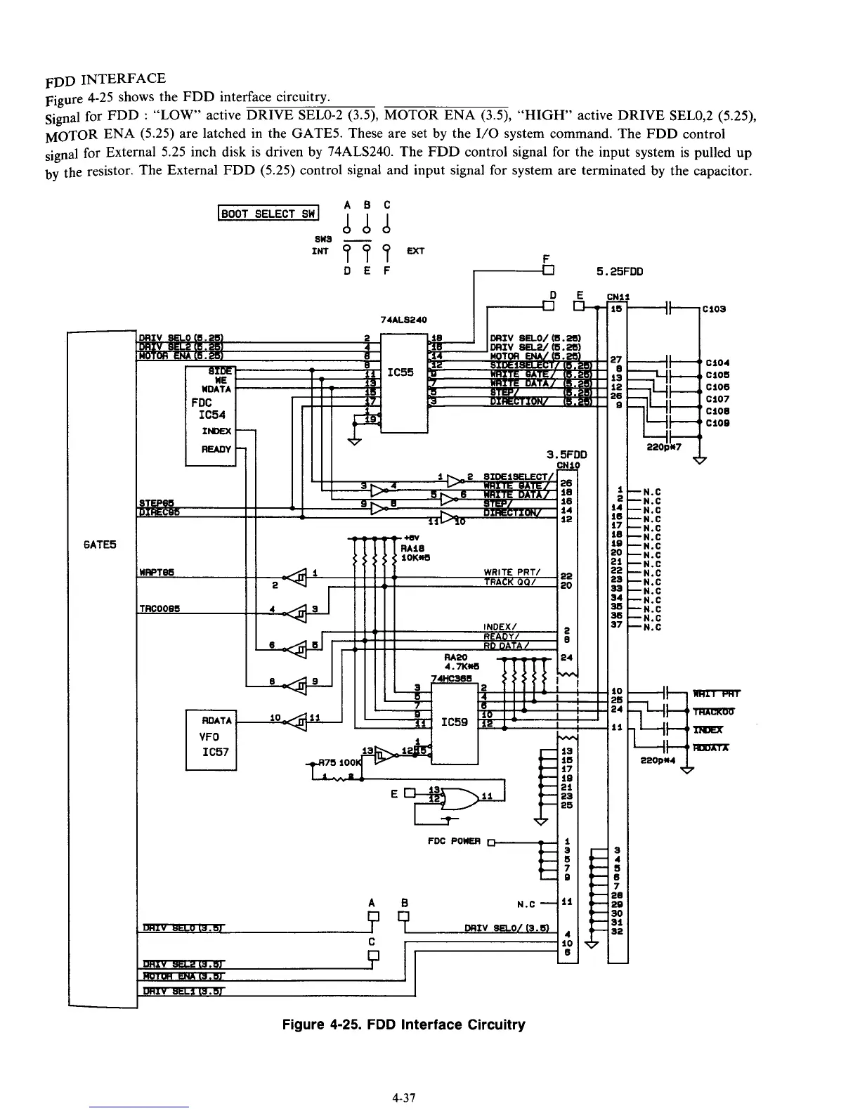
FDD INTERFACE
Figure 4-25 shows the FDD interface circuitry.
Signal for FDD
:
“LOW” active DRIVE SELO-2
(3.5),
MOTOR ENA
(3.5),
“HIGH”
active DRIVE SEL0,2 (5.25),
MOTOR ENA
(5.25)
are latched in the GATES. These are set by the
I/O
system command. The FDD control
signal for External 5.25 inch disk is driven by 74ALS240. The FDD control signal for the input system is pulled up
by
the resistor. The External FDD (5.25) control signal and input signal for system are terminated by the capacitor.
]BOOT
SELECT
sw
I
8113
-
IN1
9
9
9
EX1
DEF
rb
5.25FDD
6ATE5
74AL8240
II I
II I
r
I
IC57
J
17
75
100
*
FDC
POW
D
A0
li
N.C
-
0
%L013.m
DRIV
SaO/
(3.6)
C
10
n
1
6
I
Figure
4-25.
FDD Interface Circuitry
L
CNI
z
.27
.a
.
13
.
12
.28
.Q
1
2
14
16
17
18
19
20
21
22
23
33
34
36
38
37
-
10
-
25
-24
28
20
30
31
32
*
-N.C
-N.C
-N.C
-N.C
-N.C
-N.C
-U.C
-N.C
-N.C
-N.C
-N.C
-N.C
-N.C
-N.C
-N.C
-N.C
4-37