IV-4.
CPU
The V20 is a CMOS 16-bit microprocessor provided with an 8/16 bit architecture and an
8
bit data bus. It has a
powerful instruction set.
1. Packed BCD operation instruction.
2. High speed multiplication/division instruction.
3. Internal memory high speed block transfer.
4.
Bit operation instruction.
5.
High speed calculation of effective addresses.
The V20 is equipped with a 20-bit address bus that can access a 1M byte memory. In addition, the V20 has
emulation functions of 8080 and comes with a standby mode that significantly reduces power consumption. The V20
can be used in two scale systems, the minimum mode, which is suitable for a small system, and the maximum mode,
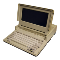
which is suitable for a large system. The microprocessor is configured in the TANDY 1400LT in the maximum
mode.
IV-5.
Clock
Generator
(Custom
IC)
This custom-made IC (IC2) is a clock pulse generator/driver for microprocessors and their peripherals using
high-speed CMOS technology. The custom-made IC has two speed MODE. The MODE is selectable by the level at
pin
1
of IC2. The custom-made IC receives
a
14.318MHz input clock and divides it by 2 to produce CPU “CLK”
(7.16MHz
:
High speed MODE), and also divides it by 3 to produce CPU “CLK” (4.77MHz
:
Normal speed
MODE). The custom-made IC also divides the same frequency by 6 and feeds the resulting 2.39MHz signal to the
peripheral circuit to be used as the “PRCLK”. In addition, to be used by the clock for DMA the custom-made IC
produces 4.77MHz “DMACLK”. The “OSC” (pin
12
of IC2) outputs a signal at the same frequency as the crystal
input. (All clocks are
50%
duty cycle)
MODE NORMAL SPEED HIGH SPEED
osc
14.318 MHz 14.318 MHz
CLK
4.77 MHz 7.16 MHz
PRCLK
2.39 MHz
2.39
MHz
DMACLK
4.77 MHz 4.77 MHz
LEVEL at Pin
1
of IC2
High
LOW
Table 4-1. Clock
Speed
When the power is turned on, the CPU and the peripheral circuits are reset by IC2 using
“
RESIN” signal (this
Schmitt-trigger input generates the “RESET” output). Reset timing is provided by
“
RESIN” input to Schmitt-
trigger input gate and flip-flop which will synchronize the reset timing to the falling edge of “CLK”.
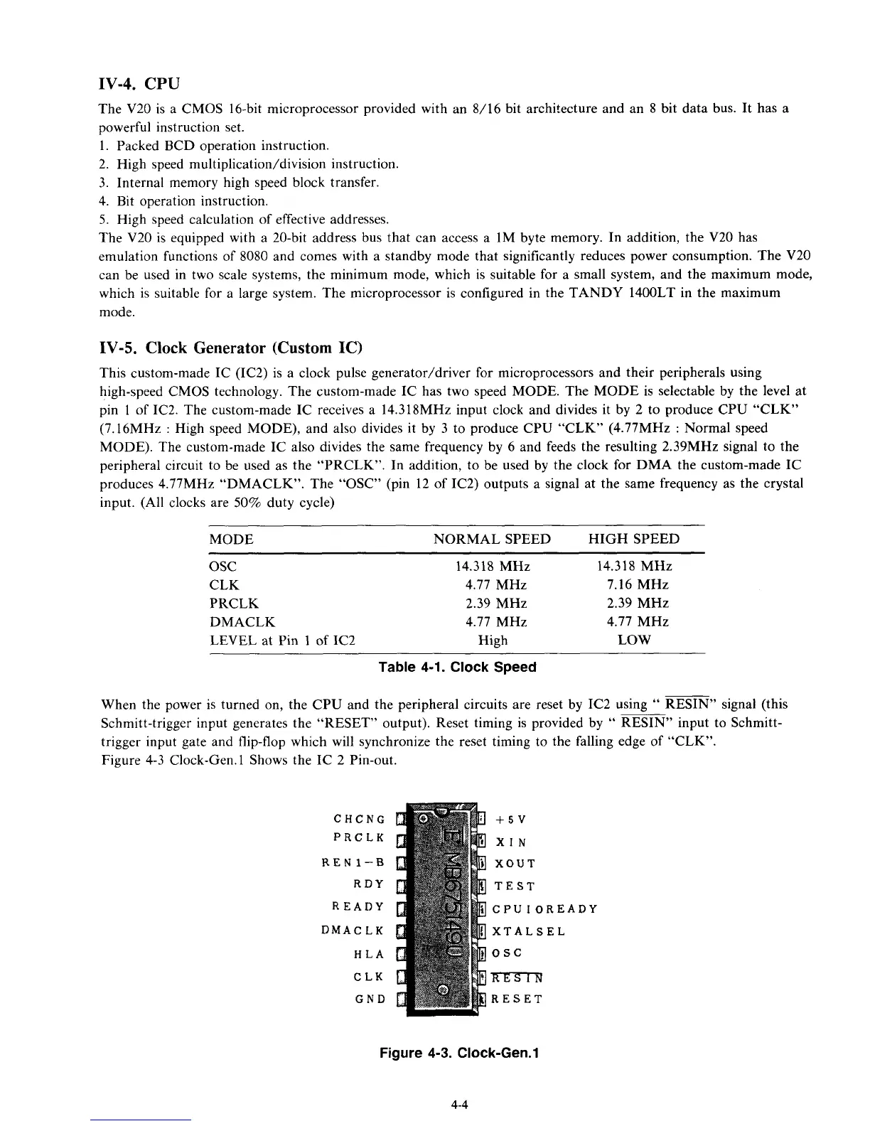
Figure 4-3 Clock-Gen.1 Shows the IC 2 Pin-out.
CHCNG
PRCLK
REN1-I3
RDY
READY
DMACLK
HLA
CLK
GND
+5v
XIN
XOUT
TEST
CPUIO
XTALS
osc
mc3-m
RESET
READY
EL
Figure
4-3. Clock-Gen.1
4-4