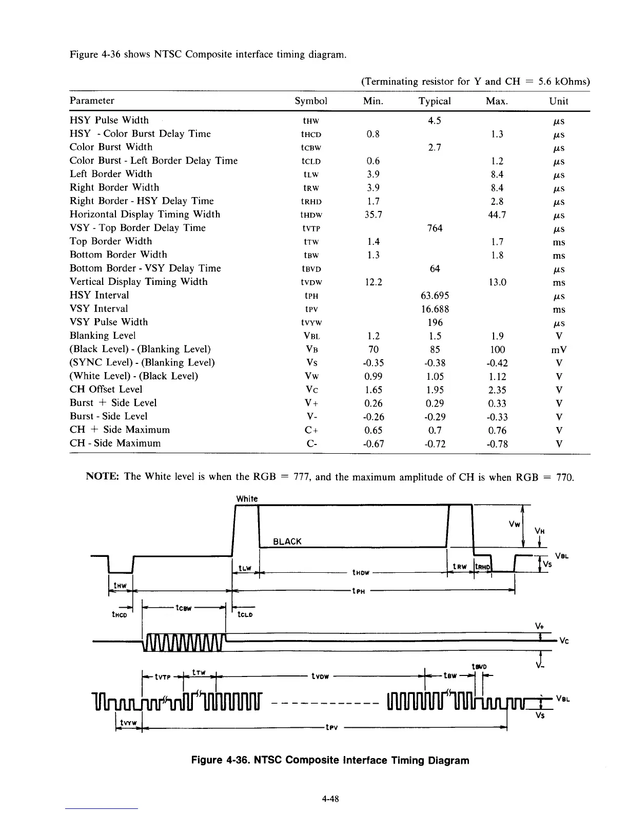
Figure 4-36 shows NTSC Composite interface timing diagram.
A
vw
VM
BLACK
vi
(Terminating resistor for Y and CH
=
5.6 kOhms)
Parameter Symbol Min. Typical Max. Unit
HSY Pulse Width
HSY
-
Color Burst Delay Time
Color Burst Width
Color Burst
-
Left Border Delay Time
Left Border Width
Right Border Width
Right Border
-
HSY Delay Time
Horizontal Display Timing Width
VSY
-
Top Border Delay Time
Top Border Width
Bottom Border Width
Bottom Border
-
VSY Delay Time
Vxrtical Display Timing Width
HSY Interval
VSY Interval
VSY Pulse Width
Blanking Level
(Black Level)
-
(Blanking Level)
(SYNC Level)
-
(Blanking Level)
(White Level)
-
(Black Level)
CH Offset Level
Burst
+
Side Level
Burst
-
Side Level
CH
+
Side Maximum
CH
-
Side Maximum
tHW
tHCD
tCBW
~CLD
tLW
tRW
tRHD
tHDW
tVTP
tTW
tBW
tBVD
tVDW
tPH
tPV
tvvw
VEL
vs
vw
vc
V+
V-
C+
C-
VB
0.8
0.6
3.9
3.9
1.7
35.7
1.4
1.3
12.2
1.2
70
-0.35
0.99
1.65
0.26
0.65
-0.26
-0.67
4.5
2.7
764
64
63.695
16.688
196
1.5
85
1.05
1.95
0.29
-0.29
0.7
-0.72
-0.3
8
1.3
1.2
8.4
8.4
2.8
44.7
1.7
1.8
13.0
1.9
100
-0.42
1.12
2.35
0.33
0.76
-0.33
-0.78
NOTE:
The White level is when the RGB
=
777, and the maximum amplitude of CH is when RGB
=
770.
V+
vc
I
Figure
4-36.
NTSC Composite Interface Timing Diagram
4-48