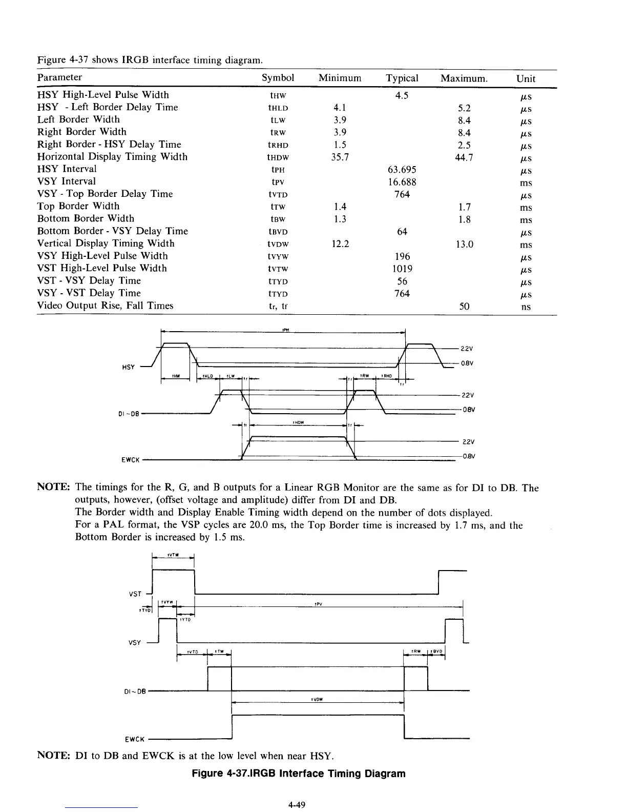
Figure 4-37 shows IRGB interface timing diagram.
1PV
tTYD
-
fYTD
Parameter Symbol Minimum Typical Maximum. Unit
HSY High-Level Pulse Width
fHW
4.5
US
Left Border Width
tLW
HSY
-
Left Border Delay Time
tHLD
Right Border Width
fRW
Right Border
-
HSY Delay Time tRHD
Horizontal Display Timing Width tHDW
HSY Interval
tPH
VSY Interval tPV
VSY
-
Top Border Delay Time tVTD
Top Border Width tTW
Bottom Border Width tBW
Bottom Border
-
VSY Delay Time
tBVD
Vertical Display Timing Width tVDW
VSY High-Level Pulse Width tvvw
VST High-Level Pulse Width tVTW
VST
-
VSY Delay Time tTYD
VSY
-
VST Delay Time tTYD
Video Output Rise, Fall Times
tr, tf
4.1
3.9
3.9
1.5
35.7
1.4
1.3
12.2
63.695
16.688
764
64
196
1019
56
764
5.2
8.4
8.4
2.5
44.7
1.7
1.8
13.0
50
HSY
DI
-DE
V
4
0.8V
EWCK
NOTE:
The timings for the
R,
G,
and B outputs for
a
Linear RGB Monitor are the same as for
DI
to DB. The
outputs, however, (offset voltage and amplitude) differ from DI and DB.
The Border width and Display Enable Timing width depend on the number of dots displayed.
For
a
PAL format, the VSP cycles are 20.0 ms, the Top Border time is increased by 1.7 ms, and the
Bottom Border is increased by 1.5
ms.
I--=---
VST
1
NOTE:
DI to DB and EWCK is at the low level when near HSY.
Figure
4-37.IRGB
Interface Timing Diagram
4-49