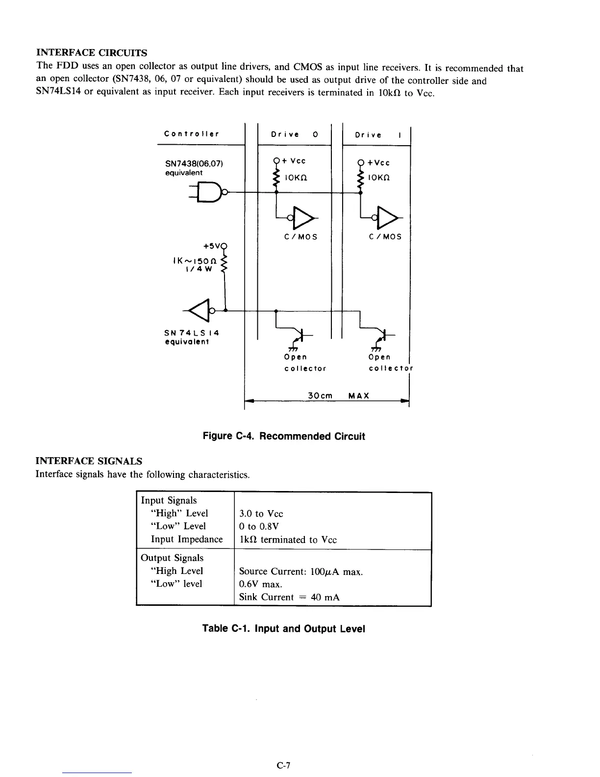
INTERFACE CIRCUITS
The
FDD
uses an open collector as output line drivers, and CMOS as input line receivers. It is recommended that
an open collector (SN7438, 06, 07 or equivalent) should be used as output drive of the controller side and
SN74LS14 or equivalent as input receiver. Each input receivers
is
terminated in lOkR to Vcc.
Drive
0
t
vcc
lOKn
C/MOS
Controller
Drive
I
C
/
MOS
SN7438(06,07)
equivalent
Input Signals
“High” Level
“Low” Level
Input Impedance
Output Signals
“High Level
“Low” level
D-
3.0 to Vcc
0
to 0.8V
lkfl terminated to Vcc
Source Current: 100pA max.
0.6V max.
Sink Current
=
40 mA
SN74LS
14
equivalent
Figure C-4. Recommended Circuit
INTERFACE SIGNALS
Interface signals have the following characteristics.
Table C-1. Input and Output Level
c-7