FDD
Control
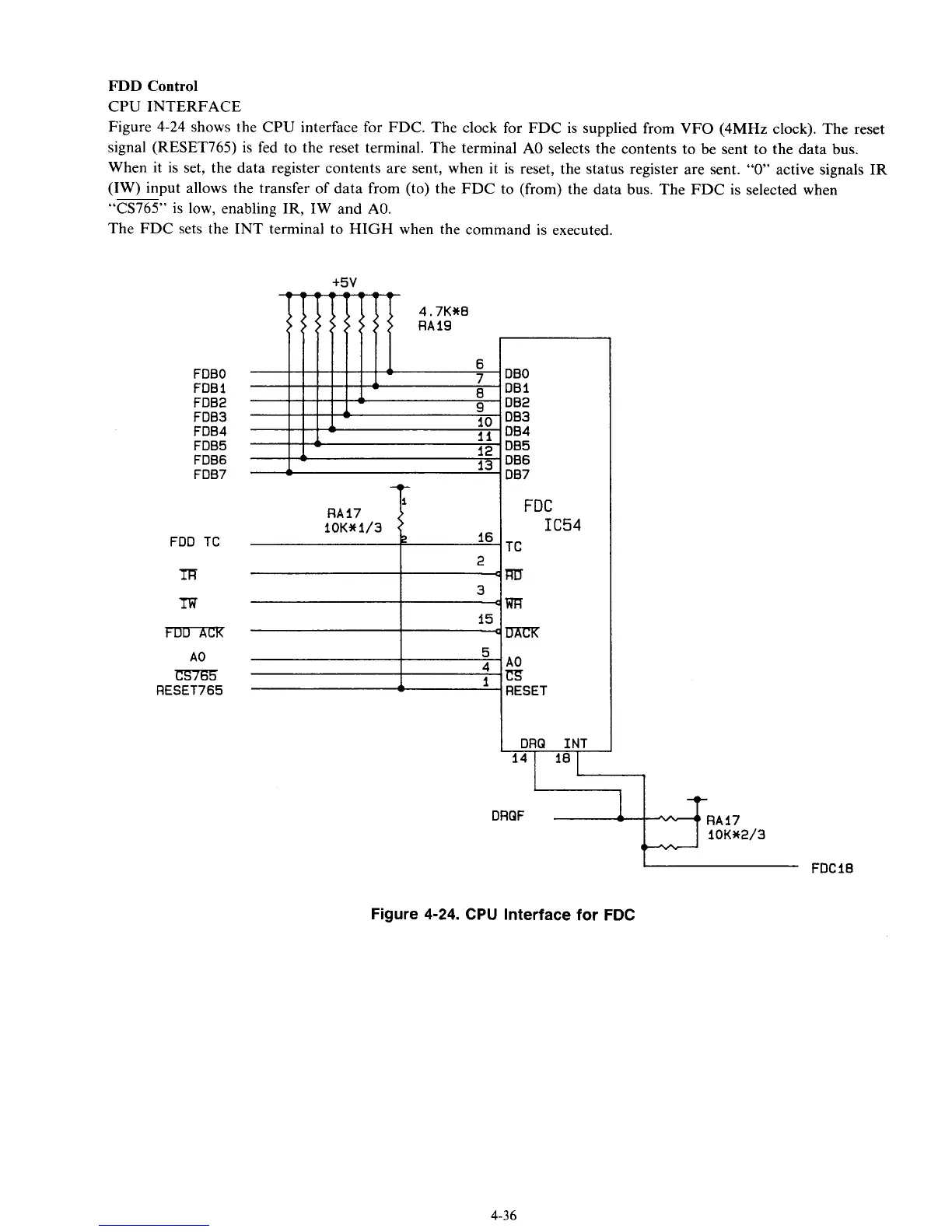
CPU
INTERFACE
Figure
4-24
shows the CPU interface for FDC. The clock for FDC is supplied from
VFO
(4MHz
clock). The reset
signal (RESET765) is fed to the reset terminal. The terminal A0 selects the contents to
be
sent to the data
bus.
When it is set, the data register contents are sent, when it is reset, the status register are sent.
“0”
active signals IR
(IW) input allows the transfer of data from (to) the FDC to (from) the data
bus.
The FDC is selected when
“(3765”
is
low, enabling IR, IW and AO.
The FDC sets the INT terminal to
HIGH
when the command is executed.
15
FDBO
FDBl
FDB2
FDB3
FDB4
FDB5
FDB6
FDB7
FDD TC
m
m
FDD-mx
A0
Ex5
RESET765
+5v
TC
A0
m
RESET
I
FDCI8
Figure
4-24.
CPU Interface for FDC
4-36