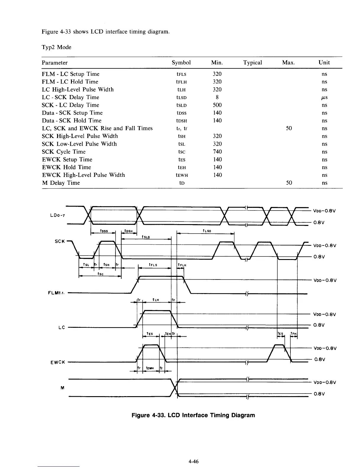
Figure 4-33 shows LCD interface timing diagram.
Typ2 Mode
Parameter Symbol Min. Typical Max. Unit
FLM
-
LC Setup Time
FLM
-
LC Hold Time
LC High-Level Pulse Width
LC
-
SCK Delay Time
SCK
-
LC Delay Time
Data
-
SCK Setup Time
Data
-
SCK Hold Time
LC, SCK and EWCK Rise and Fall Times
SCK High-Level Pulse Width
SCK Low-Level Pulse Width
SCK Cycle Time
EWCK Setup Time
EWCK Hold Time
EWCK High-Level Pulse Width
M Delay Time
tFLS
tFLH
tLH
tLSD
tSLD
tDSS
tDSH
tr, tf
tSH
tSL
tSC
tES
tEH
tEWH
tD
3
20
3
20
320
8
500
140
140
320
3 20
740
140
140
140
ns
ns
ns
PS
ns
ns
ns
50
ns
ns
ns
ns
ns
ns
ns
50
ns
SC
K
voo-0.8V
0.8V
VOD
-0.8V
FL
M
t.1.
voo-0.8V
0.8V
LC
voo-o.av
0.8V
EWCK
Figure 4-33. LCD Interface Timing Diagram
4-46