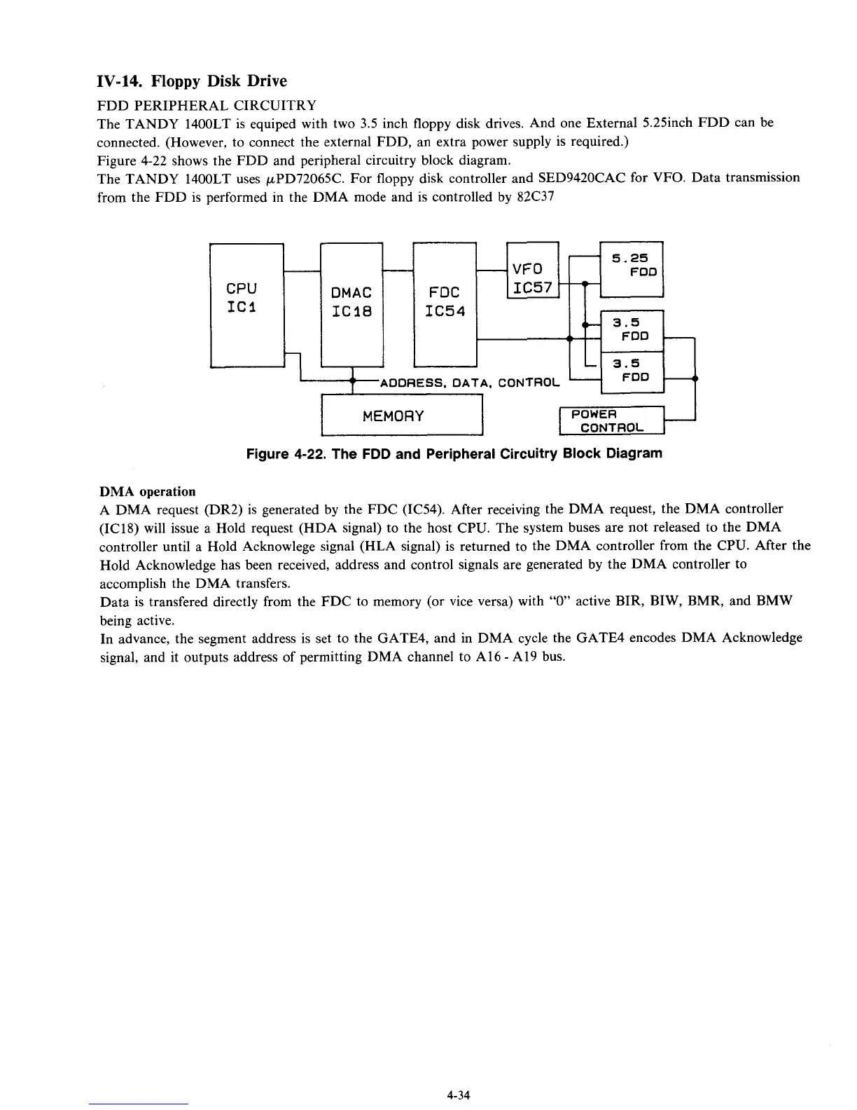
IV-14.
Floppy
Disk
Drive
FDD PERIPHERAL CIRCUITRY
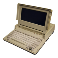
The TANDY 1400LT is equiped with two 3.5 inch floppy disk drives. And one External 5.25inch FDD can be
connected. (However, to connect the external FDD, an extra power supply is required.)
Figure 4-22 shows the FDD and peripheral circuitry block diagram.
The TANDY 1400LT uses pPD72065C. For floppy disk controller and SED9420CAC for VFO. Data transmission
from the FDD
is
performed in the DMA mode and is controlled by 82C37
FDC IC571
’
1
I
IC54
r
(C
3.5
+--
FDD
-
-
-
3.5
1
I
ADDRESS, DATA,
CONTROL
i
MEMORY
POWER
Figure
4-22.
The FDD and Peripheral Circuitry Block Diagram
DMA
operation
A DMA request (DR2) is generated by the FDC (IC54). After receiving the DMA request, the DMA controller
(IC18) will issue a Hold request (HDA signal) to the host CPU. The system buses are not released to the DMA
controller until a Hold Acknowlege signal (HLA signal) is returned to the DMA controller from the CPU. After the
Hold Acknowledge has been received, address and control signals are generated by the DMA controller to
accomplish the DMA transfers.
Data is transfered directly from the FDC to memory (or vice versa) with
“0”
active BIR, BIW, BMR, and BMW
being active.
In advance, the segment address is set to the GATE4, and in DMA cycle the GATE4 encodes DMA Acknowledge
signal, and it outputs address of permitting DMA channel to A16
-
A19 bus.
4-34