MOTOR
ON
L
DIRECTION
WRITE
DATA
- -
Ius
min
-
-
r-
-
-
6ms rnin
r
_.
ZP-
I
ps
min
-
250- 2
100
ns
21ms rnin
0
I
-
4
_-
5
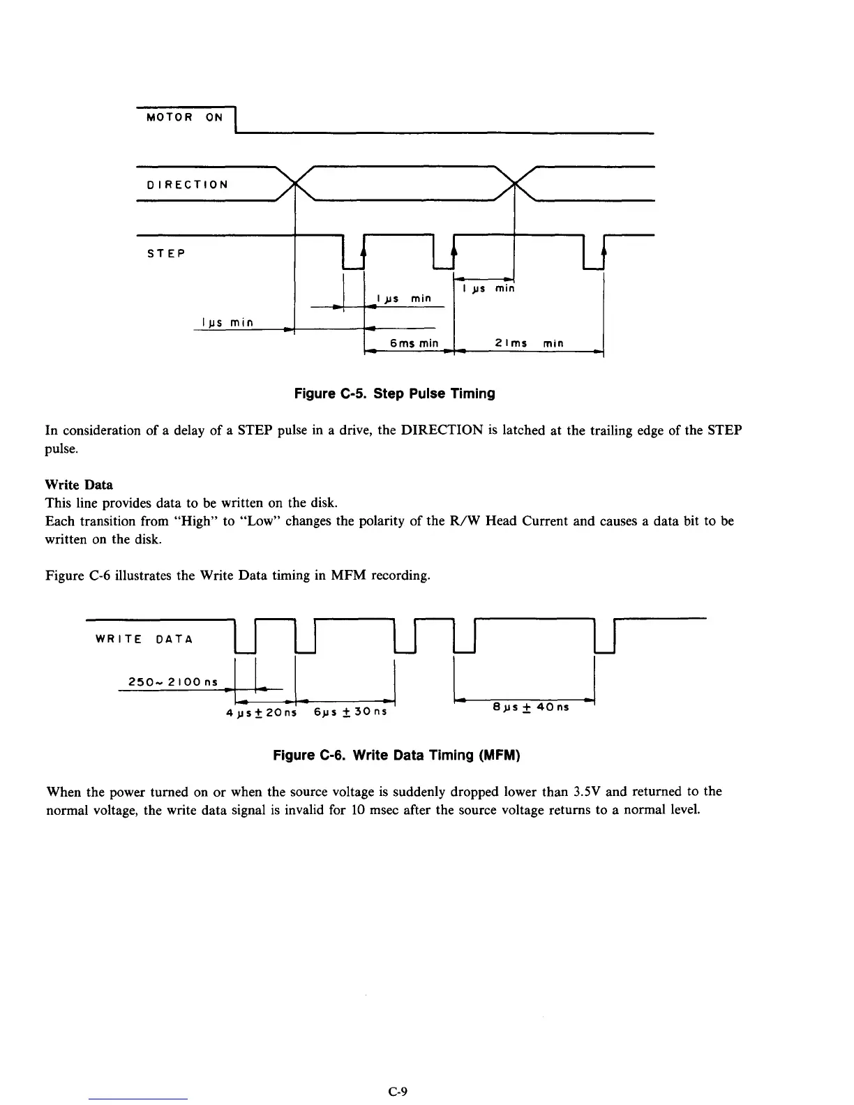
Figure C-5. Step Pulse Timing
In consideration of a delay of a STEP pulse in a drive, the DIRECTION
is
latched at the trailing edge of the STEP
pulse.
Write
Data
This line provides data to be written on the disk.
Each transition from “High” to “Low” changes the polarity of the R/W Head Current and causes a data bit to be
written on the disk.
Figure C-6 illustrates the Write Data timing in MFM recording.
Figure
C-6.
Write Data Timing
(MFM)
When the power turned on or when the source voltage is suddenly dropped lower than
3.5V
and returned to the
normal voltage, the write data signal is invalid for
10
msec after the source voltage returns to a normal level.
c-9