Figure
Number
List
of
Illustrations
DESCRIPTION
Page
Number
1-1
1-2
1-3
1-4
1-5
1-6
2- 1
2-2
2-3
2-4
2-5
2-6
2-7
2-8
2-9
2-1
0
2-1 1
2-1 2
2-1 3
2-1 4
2-1
5
2-1 6
2-1 7
2-1 8
2-1 9
2-20
2-2 1
2-22
2-23
2-24
3-1
4-1
4-2
4-3
4-4
4-5
4-6
4-7
4-8
4-9
4-1
0
4-1 1
4-1 2
4-1 3
4-1 4
4-1
5
4-1 6
4-1 7
4-1 8
4-1 9
4-20
4-21
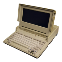
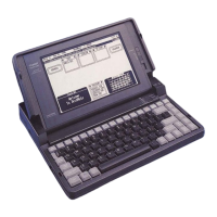
Front View
.......................................................................................................................................................
1-3
Rear View
........................................................................................................................................................
1-3
Main PCB
.........................................................................................................................................................
1-4
Power PCB
......................................................................................................................................................
1-5
Memory PCB
...................................................................................................................................................
1-6
Case Screw Removal
....................................................................................................................................
2-1
Top Case Removal
........................................................................................................................................
2-2
Cable Removal
...............................................................................................................................................
2-2
Battery Cover and Rear Cover Removal
....................................................................................................
2-3
Lever Spring Removal
...................................................................................................................................
2-3
Top Cover Removal
.......................................................................................................................................
2-4
Exploded View of LCD Assembly
.................................................................................................................
2-5
Cable Cover and LCD Removal
...................................................................................................................
2-5
Arm Assembly Removal
................................................................................................................................
2-6
LED PCB and Keyboard Removal
...............................................................................................................
2-6
Battery Connector Removal
..........................................................................................................................
2-7
Right side of Base Frame
.............................................................................................................................
2-7
Left Side
of
Base Frame
...............................................................................................................................
2-8
Connector Locations
......................................................................................................................................
2-8
Power Switch cord Removal
.........................................................................................................................
2-9
FDD Removal
.................................................................................................................................................
2-9
Exploded View
of
Power Source Assembly
................................................................................................
2-10
Bottom View of Base Frame
........................................................................................................................
2-11
Contrast knob Removal
.................................................................................................................................
2-12
Speaker Removal
...........................................................................................................................................
2-12
Exploded View
of
Main PCB Assembly
.......................................................................................................
2-13
Bottom Case Dismantling
..............................................................................................................................
2-14
Battery Pack Replacement
...........................................................................................................................
2-15
Frequency Adjustment
...................................................................................................................................
3-1
Organization of Section IV
............................................................................................................................
4-1
Block Diagram
.................................................................................................................................................
4-2
CLOCK-GEN.1
................................................................................................................................................
4-4
CLOCK-GEN.2
................................................................................................................................................
4-5
CLOCK-GEN.3
................................................................................................................................................
4-5
CLOCK-GEN.4
................................................................................................................................................
4-6
MEMORY-MAP
...............................................................................................................................................
4-7
DIP-SW Location
............................................................................................................................................
4-7
DIP-SW
............................................................................................................................................................
4-7
RAM-1
..............................................................................................................................................................
4-8
RAM-2
..............................................................................................................................................................
4-8
RAM-3
..............................................................................................................................................................
4-9
MEMORY-CARD
.............................................................................................................................................
4-10
LCD PCB
.........................................................................................................................................................
1-6
Lever Disengagement
....................................................................................................................................
2-1
ROM Address Decoder Circuit
.....................................................................................................................
4-11
ROM and Peripheral Circuitry
.......................................................................................................................
4-11
71 059C and Peripheral Circuitry
...................................................................................................................
4-15
KEYBOARD-1 (The Block Diagram in the GATE 4)
..................................................................................
4-16
KEYBOARD-2 (IC50 and Peripheral Circuitry)
............................................................................................
4-16
KEYBOARD-3 (Internal Keyboard Specification)
.......................................................................................
4-17
KEYBOARD-4 (Position, Layout and Matrix)
..............................................................................................
4-18
KEYBOARD-5 (The External Keyboard Interface Circuit and Timing Diagram
......................................
4-30
V