245
D B W R P
S
D
1
2
M
3
○
FNC
91
○○○
X Y M S
D.b R.b
KnX KnY
KnM KnS
T C
D,R
V,Z
UnG
K,H
E
" $"
DBWRP D1000 D0 K100
X20
S
D
n
S
D
n
n
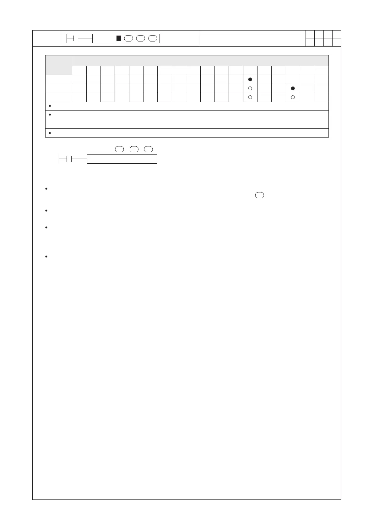
Operand
Devices
Write Data Into Data Bank
S is a 16-bit component, but when uses V, Z index to modify, that occupies a pair of V, Z index registers.
D is a 32-bit component, D = 0~655,359
When D designates to D or R as the object, that occupies 2 registers.
When D uses K or H and modies by V, Z index, that occupies a pair of V, Z index registers.
n = 1~32,767
S : the initial register ID number for a group of data
that writes to the Data Bank
D : the initial address number at the Data Bank to be
write
n : the length of the data to be write
When X20 = “OFF” → “ON” and (D1,D0) = 100, it will execute to read a group of data at the Main Unit's D1000~
D1099 and store the data into the addresses 100~199 in the Data Bank. Due to the = 100, it will write a group
data that contents with 100 words.
When a Main Unit is equipped with a VS-MC or VS-MCR memory card, it will be provided with the Data Bank. After
that, for the application which need to store or get a large number of data is convenient.
The Data Bank in the VS-MC or VS-MCR card is stored in the component of Flash ROM. Even though, in every
section of the memory, the rewrite operate is available to be used more than 10,000 times. But, it still has the limit.
So, when the program using this DBWR instruction to rewrite data into the card, better change it to the DBWRP
instruction. The DBWRP can avoid useless operate of rewrite, and then extend the lifespan of the Flash ROM.
When the instruction rewrites data to the memory card, every section (128 words) needs 15ms to execute the
function. The CPU will wait for the execution to complete and then continuously perform the rest of the program.
At that moment, the current value of the Watch Dog Timer will be automatically extended. Thus, when using this
instruction to store a large amount of data, should pay attention to the effect which write action may cause.
n
 Loading...