A20 User Manual (Revision 1.2) Copyright © 2013 Allwinner Technology Co., Ltd. All Rights Reserved. Page 590 / 812
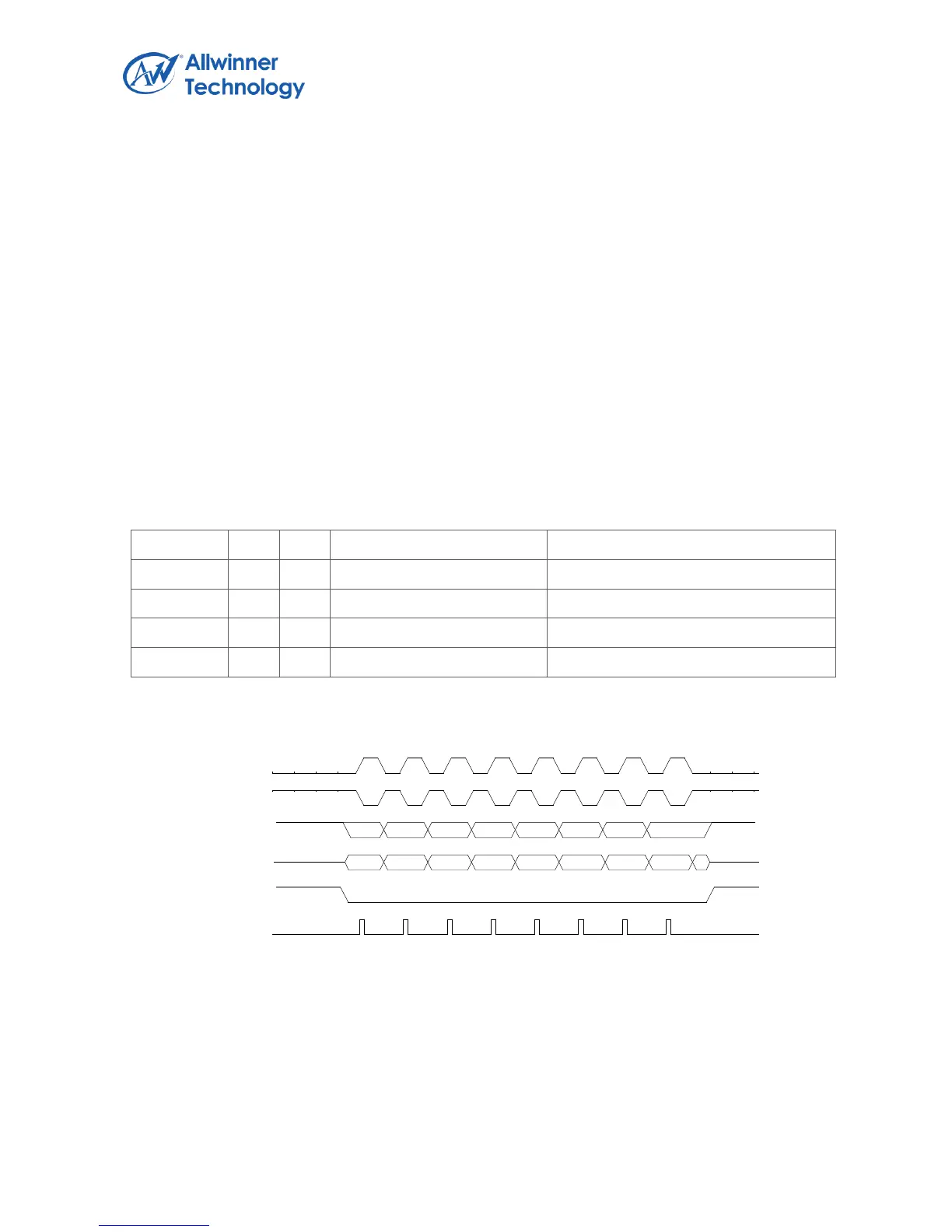
6.3.2. SPI Timing Diagram
The serial peripheral interface master uses the SPI_SCLK signal to transfer data in and out of the
shift register. Data is clocked using any one of four programmable clock phase and polarity
combinations.
During Phase 0, Polarity 0 and Phase 1, Polarity 1 operations, output data changes on the falling
clock edge and input data is shifted in on the rising edge.
During Phase 1, Polarity 0 and Phase 0, Polarity 1 operations, output data changes on the rising
edges of the clock and is shifted in on falling edges.
The POL defines the signal polarity when SPI_SCLK is in idle state. The SPI_SCLK is high level
when POL is ‘1’ and it is low level when POL is ‘0’. The PHA decides whether the leading edge of
SPI_SCLK is used for setup or sample data. The leading edge is used for setup data when PHA is ‘1’
and for sample data when PHA is ‘0’. The four kind of modes are listed below: