A20 User Manual (Revision 1.2) Copyright © 2013 Allwinner Technology Co., Ltd. All Rights Reserved. Page 103 / 812
1.8.2. PWM Register List
PWM Channel 0 Period Register
PWM Channel 1 Period Register
1.8.3. PWM Register Description
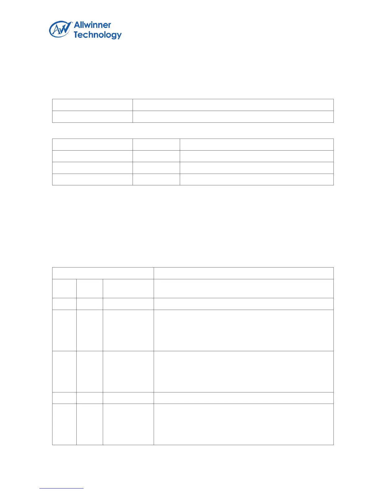
1.8.3.1. PWM CONTROL REGISTER(DEFAULT: 0X00000000)
Register Name: PWM_CTRL_REG
PWM1_RDY.
PWM1 period register ready.
0: PWM1 period register is ready to write,
1: PWM1 period register is busy.
PWM0_RDY.
PWM0 period register ready.
0: PWM0 period register is ready to write,
1: PWM0 period register is busy.
PWM1_BYPASS.
PWM CH1 bypass enable.
If the bit is set to 1, PWM1’s output is OSC24MHz.
0: disable